News Posts matching #N7P

Return to Keyword Browsing

TSMC Ships its 1 Billionth 7nm Chip

In a bid to show off its volume production prowess and technological edge (but mostly to rub it in to rival fabs), TSMC on Thursday announced that it shipped its 1 billionth chip fabricated on its 7 nm process. If these dies were combined into one big rectangular wafer, they would cover 13 New York City blocks. TSMC's 7 nm process debuted with its N7 node, which went into volume production in April 2018, over two years ago. The fab has since mass-produced 7 nm chips for the likes of Qualcomm, Apple, and AMD, among dozens of other clients. The company now looks to monetize refinements of N7, namely the N7e and N7P (DUV refinements), while executing its crucial EUV-based N7+ node, leading up to future nodelets such as N6. Much of TSMC's growth will be propelled by 5G modems, application processors, and its pivotal role in the growth of companies such as AMD.

TSMC Allocation the Next Battleground for Intel, AMD, and Possibly NVIDIA

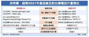
With its own 7 nm-class silicon fabrication node nowhere in sight for its processors, at least not until 2022-23, Intel is seeking out third-party semiconductor foundries to support its ambitious discrete GPU and scalar compute processor lineup under the Xe brand. A Taiwanese newspaper article interpreted by Chiakokhua provides a fascinating insight to the the new precious resource in the high-technology industry - allocation.

TSMC is one of these foundries, and will give Intel access to a refined 7 nm-class node, either the N7P or N7+, for some of its Xe scalar compute processors. The company could also seek out nodelets such as the N6. Trouble is, Intel will be locking horns with the likes of AMD for precious foundry allocation. NVIDIA too has secured a certain allocation of TSMC 7 nm for some of its upcoming "Ampere" GPUs. Sources tell China Times that TSMC will commence mass-production of Intel silicon as early as 2021, on either N7P, N7+, or N6. Business from Intel is timely for TSMC as it is losing orders from HiSilicon (Huawei) in wake of the prevailing geopolitical climate.

AMD RDNA2 "Navi 21" GPU to Double CU Count Over "Navi 10"

AMD's RDNA2 graphics architecture, which sees real-time ray-tracing among other DirectX 12 Ultimate features, could see the company double the amount of stream processors generation-over-generation, according to a specs leak by _rogame. The increase in stream processors would fall in line with AMD's effort to increase performance/Watt by 50%. It may appear like the resulting SKUs finally measure up to the likes of the RTX 2080 Ti, but AMD has GeForce "Ampere" in its competitive calculus, and should the recent specs reveal hold up, the new "Navi 21" could end up being a performance-segment competitor to GeForce graphics cards based on the "GA104" ("TU104" successor), rather than a flagship-killer.

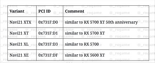
The RDNA2-based "Navi 21" GPU allegedly features 80 RDNA2 compute units amounting to 5,120 stream processors. AMD might tap into a refined 7 nm-class silicon fabrication node by TSMC to build these chips, either N7P or N7+. The die-size could measure up to 505 mm², and AMD could aim for a 50% performance/Watt gain over the "Navi 10." AMD could carve out as many as 10 SKUs out of the "Navi 21," but only three are relevant to the gamers. The SKU with the PCI device ID "0x731F: D1" succeeds the RX 5700 XT. The one bearing "0x731F: D3" succeeds the RX 5700, with a variant name "Navi 21 XL." The "Navi 21 XE" variant has a PCI ID of "0x731F: DF," and succeeds the RX 5600 XT.

Possible AMD "Vermeer" Clock Speeds Hint at IPC Gain

The bulk of AMD's 4th generation Ryzen desktop processors will comprise of "Vermeer," a high core-count socket AM4 processor and successor to the current-generation "Matisse." These chips combine up to two "Zen 3" CCDs with a cIOD (client I/O controller die). While the maximum core count of each chiplet isn't known, they will implement the "Zen 3" microarchitecture, which reportedly does away with CCX to get all cores on the CCD to share a single large L3 cache, this is expected to bring about improved inter-core latencies. AMD's generational IPC uplifting efforts could also include improving bandwidth between the various on-die components (something we saw signs of in the "Zen 2" based "Renoir"). The company is also expected to leverage a newer 7 nm-class silicon fabrication node at TSMC (either N7P or N7+), to increase clock speeds - or so we thought.

An Igor's Lab report points to the possibility of AMD gunning for efficiency, by letting the IPC gains handle the bulk of Vermeer's competitiveness against Intel's offerings, not clock-speeds. The report decodes OPNs (ordering part numbers) of two upcoming Vermeer parts, one 8-core and the other 16-core. While the 8-core part has some generational clock speed increases (by around 200 MHz on the base clock), the 16-core part has lower max boost clock speeds than the 3950X. Then again, the OPNs reference A0 revision, which could mean that these are engineering samples that will help AMD's ecosystem partners to build their products around these processors (think motherboard- or memory vendors), and that the retail product could come with higher clock speeds after all. We'll find out in September, when AMD is expected to debut its 4th generation Ryzen desktop processor family, around the same time NVIDIA launches GeForce "Ampere."
Return to Keyword Browsing
Dec 22nd, 2024 10:53 EST change timezone

New Forum Posts

Popular Reviews

Controversial News Posts