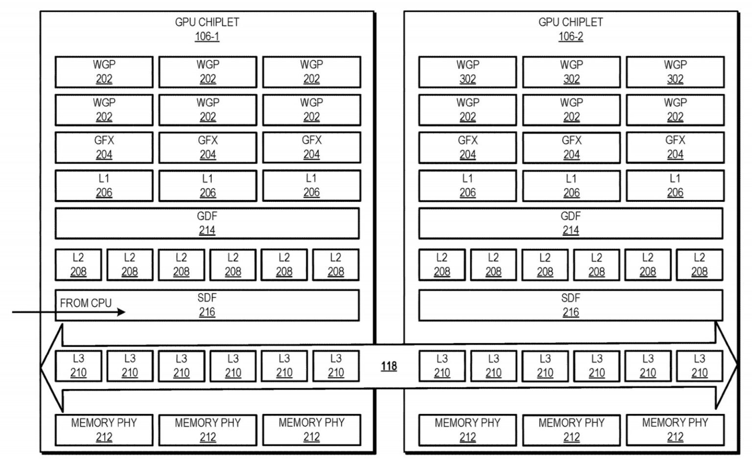
News Posts matching #Patents

Return to Keyword Browsing

Chinese Memory Manufacturer YMTC Sues Micron Over 3D NAND Patents

Chinese memory manufacturer YMTC has filed a lawsuit against U.S.-based Micron in California, alleging infringement of 11 patents related to 3D NAND Flash and DRAM products. YMTC seeks to halt Micron's sales of the allegedly infringing products in the U.S. and demands royalty payments. Founded in Wuhan, China, in 2016, YMTC is a key player in China's efforts to develop a domestic chip industry. However, in October 2022, the U.S. government placed YMTC on its Entity List, restricting its access to advanced U.S. manufacturing equipment for 3D NAND chips with 128 layers or more.

Before these restrictions, YMTC had obtained certification from Apple for its 128-layer 3D NAND chips, with the US tech giant considering using YMTC chips to reduce costs and diversify its supply chain beyond Samsung, SK Hynix and Micron. The lawsuit specifically targets Micron's 3D NAND Flash products with 96, 128, 176, and 232 layers, as well as certain DDR5 SDRAM products. This legal action follows a similar suit filed by YMTC against Micron in November, alleging infringement of eight U.S. patents related to 3D NAND Flash. With government backing, Chinese firms are increasingly engaging in patent litigation both domestically and internationally. Last year alone, Chinese courts handled over 5,000 technical intellectual property and monopoly cases.

FT Claims Arm Engineers Working on Proprietary Chip

The Financial Times this weekend has published details about an interesting development project that is currently in-the-works at British semiconductor specialist firm Arm Ltd. The article states that several executives in the industry have divulged (anonymously) that Arm's engineering team is designing a proprietary chip - these insider sources opine that this new creation could be one of the company's most advanced undertakings. The SoftBank-owned chipmaker is having a bumper year in terms of financial success and has invested in its future - it is speculated that their own semiconductor design will be showcased as a prototype product to potential new clients - with the main goal being to drum up more business and growth. Parent group SoftBank is likely pushing for maximum profit margins as it prepares Arm for an initial public offering (IPO) this year.

Arm's modus operandi involves partnering up with other chip manufacturers in order to license out its semiconductor intellectual properties. In turn these partners are expected to deal with the overall design and manufacturing processes of chips (plus sales of). Arm has teamed up with foundries TSMC and Samsung in the past to create prototypes for software testing purposes, but not much has been heard about those proofing projects in the following years. In an unusual turn (from certain industry perspectives) from its traditional working methodologies, it seems that Arm is embracing a different approach by producing its own compelling designs, with the hope of demonstrating greater potential to customers. FT's sources have provided evidence that Arm has expanded its operations and that a newly formed "solutions engineering" team is focused on prototyping new silicon for usage in mobile hardware and related devices.

AMD Patents Chiplet-based GPU Design With Active Cache Bridge

AMD on April 1st published a new patent application that seems to show the way its chiplet GPU design is moving towards. Before you say it, it's a patent application; there's no possibility for an April Fool's joke on this sort of move. The new patent develops on AMD's previous one, which only featured a passive bridge connecting the different GPU chiplets and their processing resources. If you want to read a slightly deeper dive of sorts on what chiplets are and why they are important for the future of graphics (and computing in general), look to this article here on TPU.

The new design interprets the active bridge connecting the chiplets as a last-level cache - think of it as L3, a unifying highway of data that is readily exposed to all the chiplets (in this patent, a three-chiplet design). It's essentially AMD's RDNA 2 Infinity Cache, though it's not only used as a cache here (and for good effect, if the Infinity Cache design on RDNA 2 and its performance uplift is anything to go by); it also serves as an active interconnect between the GPU chiplets that allow for the exchange and synchronization of information, whenever and however required. This also allows for the registry and cache to be exposed as a unified block for developers, abstracting them from having to program towards a system with a tri-way cache design. There are also of course yield benefits to be taken here, as there are with AMD's Zen chiplet designs, and the ability to scale up performance without any monolithic designs that are heavy in power requirements. The integrated, active cache bridge would also certainly help in reducing latency and maintaining chiplet processing coherency.
AMD Chiplet Design Patent with Active Cache Hierarchy AMD Chiplet Design Patent with Active Cache Hierarchy AMD Chiplet Design Patent with Active Cache Hierarchy AMD Chiplet Design Patent with Active Cache Hierarchy

Intel Accused of Infringing FinFET Patents of the Microelectronics Institute of the Chinese Academy of Sciences

Today we are finding out that Intel has allegedly infringed FinFET patents of Microelectronics Institute of the Chinese Academy of Sciences. On July 28th, the patent review committee has heard an application that accuses Intel of violating a patent 201110240931.5 commonly referred to as FinFET patent. The patent dates back to 2011, and it comes from the Chinese Academy of Sciences, mainly Microelectronics Institute. The Chinese patent holders are asking for as much as 200 million yuan, which roughly translates to 28,664,380 US dollars. Given that this patent infringement is a major one for Intel, it is sure that a company will be pursued extensively in court. All of the Intel's semiconductors use FinFET technology, and if this is true, the violation is rather big. For more in detail reading, please refer to the source which goes through the history of Intel and Microelectronics Institute patent violation filing.
Intel 3rd generation FInFETs

TSMC Files Complaints Against GlobalFoundries for Infringement of 25 Patents

TSMC, the world's leading global innovator in semiconductor manufacturing, filed multiple lawsuits on September 30, 2019 against GlobalFoundries in the United States, Germany and Singapore for its ongoing infringement of 25 TSMC patents by at least its 40nm, 28nm, 22nm, 14nm, and 12nm node processes. In the complaints, TSMC demands injunctions to stop GlobalFoundries' manufacture and sale of infringing semiconductor products. TSMC also seeks substantial monetary damages from GlobalFoundries for its sale of infringing semiconductor products and unlawful use of TSMC's patented semiconductor technologies.

The 25 TSMC patents in the complaints relate to a diverse set of technologies, including FinFET designs, shallow trench isolation techniques, double patterning methods, advanced seal rings and gate structures, and innovative contact etch stop layer designs. These specific technologies cover the core features of mature and advanced semiconductor manufacturing processes. The patents at issue comprise just a small portion of TSMC's extensive portfolio that numbers more than 37,000 granted patents worldwide. TSMC was ranked one of the top 10 companies for U.S. patent grants last year, for the third consecutive year.

AMD Wins Back Three Graphics Patents from LG

AMD won back ownership of three graphics patents that had earlier been struck down on a complaint by LG Electronics. A U.S. Court of Appeals for the Federal Circuit overruled a ruling of the Patent Trial and Appeal Board (PTAB) which observed that AMD subsidiary ATI Technologies ULC (now reorganized as RTG), has a claim to U.S. patents numbered 7,742,053, 6,897,871, and 7,327,369. The three patents deal with critical technology related to Unified Shaders.

The PTAB had earlier dismissed ATI's ownership of the patents on grounds that the IP claimed was "too obvious in light of prior art." A bench of three Judges in a unanimous decision ruled that ATI had "had conceived of their inventions before the prior art." Put simply, the court was satisfied that the technologies protected by these patents were invented by ATI before the "prior art," and were not "obvious next steps" to it.

Microsoft Joins the Open Invention Network, Adds 60,000 Patents To Protect Linux and Open Source

Steve Ballmer once said 'Linux is a cancer'. Times have changed a lot, and since Satya Nadella became CEO of Microsoft, Linux and Open Source have become really important for Redmond's company. Azure is based on Linux, for example, and this OS dominates the cloud platform with about half of Azure VMs being Linux ones). Running Linux distributions such as Ubuntu, SuSE or Fedora is also possible natively under Windows 10 through Windows Subsystem for Linux.

The company has made big strategic acquisitions, and Microsoft recently acquired Github, but that approach to Linux and Open Source goes further with the new announcement. Microsoft has joined the Open Invention Network (OIN), a consortium that defines itself as a "shared defensive patent pool with the mission to protect Linux". With that move, Microsoft is bringing 60,000 patents to OIN that will be available royalty-free to anyone who joins the OIN community.
Return to Keyword Browsing
Jul 25th, 2024 18:22 EDT change timezone

New Forum Posts

Popular Reviews

Controversial News Posts