News Posts matching #Samsung

Return to Keyword Browsing

First Intel "Lakefield" Powered Samsung Galaxy Book S Listed on the Company's Canadian Store

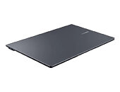
One of the first Intel "Lakefield" heterogenous processor-powered devices, a Samsung Galaxy Book S model, is listed by Samsung on its Canadian online store. The Galaxy Book series typically consists of Arm-powered clamshell/convertible notebooks that use Windows 10 (Arm version). The device in question is a Galaxy Book S 13.3-inch notebook bearing model number NP767XCM-K01CA, and comes in two color trims - "Mercury Gray" and "Earthy Gold."

Under the hood is an Intel Core i5-L16G7 "Lakefield" heterogenous processor that has four "Tremont" low-power cores, and a "Sunny Cove" high-performance cores, in an arrangement rivaling Arm big.LITTLE, the first of many such chips from the company, as it taps into new technologies such as heterogenous cores and advanced Foveros chip packaging to design its future processors. The notebook offers Full HD resolution, 8 GB of RAM, 256 GB or 512 GB of solid-state NVMe storage, 802.11ax 2x2 WLAN, and a 42 Wh battery, possibly with double-digit hour battery life. All of this goes into a 6.2 mm (folded) device weighing under a kilogram.

Samsung Expands its Foundry Capacity with A New Production Line in Pyeongtaek

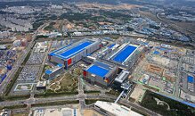
Samsung Electronics Co., Ltd., a world leader in advanced semiconductor technology, today announced plans to boost its foundry capacity at the company's new production line in Pyeongtaek, Korea, to meet growing global demand for cutting-edge extreme ultraviolet (EUV) solutions.

The new foundry line, which will focus on EUV-based 5 nanometer (nm) and below process technology, has just commenced construction this month and is expected to be in full operation in the second half of 2021. It will play a pivotal role as Samsung aims to expand the use of state-of-the-art process technologies across a myriad of current and next generation applications, including 5G, high-performance computing (HPC) and artificial intelligence (AI).

Samsung T7 Portable SSD is Now Available for Purchase

Following the release of Samsung's T7 Touch portable SSD in January, the T7 is now available. Samsung T7 combines sleek, compact design with the fastest transfer speeds currently available based on the USB 3.2 Gen 2 standard. The business card-sized portable SSD can be slipped into nearly any pocket and holds up to 2 TB of data. Samsung T7 is the perfect everyday storage companion for those looking to save video and photo content from a variety of USB-compatible devices. The T7 saves time with incredibly fast transfer speeds, and gives users peace of mind with data security features.

The T7 offers a significant speed upgrade over previous storage solutions. With a read speed of 1,050 MB/s and a write speed of 1,000 MB/s, it is approximately twice as fast as its predecessor, the T5, and up to 9.5 times faster than external hard disk drives. Moreover, the device can reach its maximum speed when used with the NVMe interface. With these speeds, Samsung T7 can help improve daily workflow and save valuable time for digital creative professionals.
Samsung T7

Samsung Unveils Innovative Storage Technology at OCP Virtual Global Summit

Samsung announced today in an OCP Virtual Summit keynote that it has developed a solid state drive (PM9A3 SSD) with a SNIA-based E1.S form factor and full PCIe Gen 4 support to harness the production efficiencies of the company's sixth-generation (1xx-layer), three-bit V-NAND. At the same time, the company said that it has introduced a comprehensive reference design for its E1.S-based storage system.

The keynote, in addition to announcing the PM9A3, highlighted a new approach to open source multi-industry storage collaboration that spotlighted the development of an open-source platform (OSP) fundamentally tied to cloud-scale infrastructure deployments. It was presented by Jongyoul Lee, senior vice president of Samsung's Memory Software Development Team at the Open Compute Project Virtual Global Summit.

NVIDIA Underestimated AMD's Efficiency Gains from Tapping into TSMC 7nm: Report

A DigiTimes premium report, interpreted by Chiakokhua, aka Retired Engineer, chronicling NVIDIA's move to contract TSMC for 7 nm and 5 nm EUV nodes for GPU manufacturing, made a startling revelation about NVIDIA's recent foundry diversification moves. Back in July 2019, a leading Korean publication confirmed NVIDIA's decision to contract Samsung for its next-generation GPU manufacturing. This was a week before AMD announced its first new-generation 7 nm products built for the TSMC N7 node, "Navi" and "Zen 2." The DigiTimes report reveals that NVIDIA underestimated the efficiency gains AMD would yield from TSMC N7.

With NVIDIA's bonhomie with Samsung underway, and Apple transitioning to TSMC N5, AMD moved in to quickly grab 7 nm-class foundry allocation and gained prominence with the Taiwanese foundry. The report also calls out a possible strategic error on NVIDIA's part. Upon realizing the efficiency gains AMD managed, NVIDIA decided to bet on TSMC again (apparently without withdrawing from its partnership with Samsung), only to find that AMD had secured a big chunk of its nodal allocation needed to support its growth in the x86 processor and discrete GPU markets. NVIDIA has hence decided to leapfrog AMD by adapting its next-generation graphics architectures to TSMC's EUV nodes, namely the N7+ and N5. The report also speaks of NVIDIA using its Samsung foundry allocation as a bargaining chip in price negotiations with TSMC, but with limited success as TSMC established its 7 nm-class industry leadership. As it stands now, NVIDIA may manufacture its 7 nm-class and 5 nm-class GPUs on both TSMC and Samsung.

Samsung/AMD Radeon GPU for Smartphones is Reportedly Beating the Competition

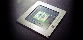
Samsung and AMD announced last year their strategic partnership to bring AMD RDNA GPUs to the Samsung mobile chips and use that as the only GPU going forward. And now, some performance numbers are going around about the new RDNA smartphone GPU that is compared to Qualcomm Adreno 650 GPU. Thanks to the South Korean technology forum "Clien", they have obtained some alleged performance results of new GPU in the GFXBench benchmark. The baseline in these tests is the Qualcomm Adreno 650 GPU, which scored 123 FPS in Manhattan 3.1 test, 53 FPS in Aztec Normal, and 20 FPS in Aztec High.

The welcome surprise here is the new RDNA GPU Samsung is pursuing. It has scored an amazing 181 FPS in Manhattan 3.1 test (up 47% from Adreno 650), 138 FPS in Aztec Normal (up almost 200% from Adreno 650), and 58 FPS in Aztec High which is 190% higher compared to Adreno 650. This performance results could be very true, as the Samsung and AMD collaboration should give first results in 2021 when the competition will be better, and they need to prepare for that. You always start designing a processor for next-generation workloads and performance if you want to be competitive by the time you release a product.
AMD RDNA GPU

Samsung to Commence 5nm EUV Mass-Production in Q2-2020, Develop 3nm GAAFET Node

Samsung in its Q1-2020 financials release disclosed that the company will commence mass production of chips on its cutting-edge 5 nanometer EUV silicon fabrication process within Q2-2020 (that's before July 2020). This is big, as it lends credence to rumors of NVIDIA secretly developing 5 nm GPUs. Suddenly, it's possible that "Ampere," if not "Hopper," is 5 nm EUV-based, as NVIDIA has chosen Samsung to be its foundry partner for next-generation GPUs.

"In the second quarter, the Company aims to expand EUV leadership, beginning with the start of mass production of 5 nm products, while closely monitoring the uncertain market situation caused by COVID-19," the company states in the release. Samsung also announced that following commencement of mass production on 5 nm, further development of GAAFET (gate all-around FET) 3 nanometer silicon fabrication process will get underway. The company appears to be erring on the side of caution with its forward-looking statements, though. Much of what Samsung does will be dictated by the impact of COVID-19 on the supply chain and market.

Samsung Electronics Announces First Quarter 2020 Results

Samsung Electronics today reported financial results for the first quarter ended March 31, 2020. Total revenue was KRW 55.33 trillion, a decrease of 7.6% from the previous quarter mainly due to weak seasonality for the Company's display business and Consumer Electronics Division and partially due to effects of COVID-19. From a year earlier, revenue rose 5.6% due to increasing demand for server and mobile components.

Operating profit was lower by KRW 0.7 trillion quarter-on-quarter to KRW 6.45 trillion, affected by the same factors that weighed on revenue with a corresponding decrease in operating margin, even though memory earnings were higher. Compared with a year earlier, operating profit increased by KRW 0.2 trillion with an improved product mix in the mobile business and additional diversification of the Company's customer base in mobile OLED.

In the quarter, foreign exchange movements had little impact on the overall operating profit as the positive effects from a stronger U.S. dollar and euro against the won - felt mainly in the component business - were offset by weakness in currencies in major emerging markets.

Origin PC Announces The Ludicrous PC: High-End Custom PC Inside a Tesla-inspired Chassis

ORIGIN PC is proud to announce the availability of a custom ORIGIN PC desktop powered by AMD Ryzen inside a Tesla Model S for kids called the LUDICROUS PC. Originally built for Marques Brownlee, also known as MKBHD, and inspired by his Tesla Model S, the LUDICROUS PC is a powerful gaming desktop featuring liquid cooling and is capable of being driven just like a normal Radio Flyer Tesla Model S. The LUDICROUS PC is available now on ORIGINPC.com with options to select the color and rims for the vehicle.

Designed by the ORIGIN PC team, the LUDICROUS PC is a special build that required some challenges to overcome such as airflow, fitting the PC parts inside the Tesla Model S for kids, and still maintaining the drivability of the car. The first LUDICROUS PC was engineered, built, and shipped to MKBHD late 2019 for the opening of his new studio in 2020. The LUDICROUS PC features working headlights, a horn, the capability of being driven forwards and backwards, and a remote that can turn the PC on.

NVIDIA is Secretly Working on a 5 nm Chip

According to the report of DigiTimes, which talked about TSMC's 5 nm silicon manufacturing node, they have reported that NVIDIA is also going to be a customer for it and they could use it in the near future. And that is very interesting information, knowing that these chips will not go in the next generation of GPUs. Why is that? Because we know that NVIDIA will utilize both TSMC and Samsung for their 7 nm manufacturing nodes for its next-generation Ampere GPUs that will end up in designs like GeForce RTX 3070 and RTX 3080 graphics cards. These designs are not what NVIDIA needs 5 nm for.

Being that NVIDIA already has a product in its pipeline that will satisfy the demand for the high-performance graphics market, maybe they are planning something that will end up being a surprise to everyone. No one knows what it is, however, the speculation (which you should take with a huge grain of salt) would be that NVIDIA is updating its Tegra SoC with the latest node. That Tegra SoC could be used in a range of mobile devices, like the Nintendo Switch, so could NVIDIA be preparing a new chip for Nintendo Switch 2?
NVIDIA Xavier SoC

Samsung Developing 160-layer 3D NAND Flash Memory

Samsung Electronics is reportedly developing its 7th generation V-NAND memory with ultra-high 3D stacking technology. The first model will feature at least 160 layers, subsequent models will feature more. In early signs of the company not wanting to yield the technological initiative to China's YMTC, the first 160-layer V-NAND by Samsung is slated to come out roughly around the time YMTC's 128-layer 3D NAND flash hits mass production, towards the end of 2020.

At the heart of the ultra-high 3D stack is Samsung's proprietary Double Stack technology. The double-stack technology creates electron holes at two separate times for current to go through circuits. The current-generation single-stack chips creates these holes once throughout the stack per cycle. The 160-layer NAND flash is expected to herald a 67% increase in densities per package over the 96-layer chips in the market. Densities could also be increased by other means such as switching to newer semiconductor fabrication nodes, and PLC (5 bits per cell), which is currently being developed by KIOXIA.

Intel Regains Top Position in Semiconductor Market

Intel has regained its position of semiconductor leader by revenue from Samsung for the 2019 period. Intel had been trailing Samsung for the last 2 years but after a decline in DRAM demand Intel reclaimed the leading position. The overall semiconductor market saw revenue drops of 12% in 2019 which hit other companies worse than Intel.

Andrew Norwood, research VP at Gartner says: "Oversupply in the DRAM market helped push the overall memory market down 32.7% 2019. The memory market accounted for 26.1% of semiconductor sales in 2019 and was the worst-performing device segment,". Samsung being a large DRAM supplier was hit hard by this compared to Intel with limited memory production. Gartner the research firm has also cut its global semiconductor market outlook this year to a 0.9% dip from the 12.5% growth estimated at the end of 2019 due to the effects of COVID-19.

ASUS Readies Zenbook 14 Model Combining Ryzen 4000 and GeForce MX350 Graphics

ASUS is giving finishing touches to the launch of a new Zenbook 14 (UX434IQ) model with a combination of a Ryzen 4000 "Renoir" processor and NVIDIA's entry-level GeForce MX350 discrete graphics. Although never pictured and with no confirmation of whether it gets the swanky ScreenPad (a color touchscreen that works like the notebook's trackpad); the combine surfaced in a Futuremark database submission.

The Zenbook 14 (UX434IQ) combines an AMD Ryzen 7 4700U (8-core/8-thread) processor with NVIDIA GeForce MX350 discrete graphics, and more interestingly, 16 GB of LPDDR4x-4266 memory. The "Pascal" based MX350 graphics features 640 CUDA cores, and a 64-bit GDDR5 memory interface holding 2 GB of memory. It's marketed to offer a 2.5x performance uplift against an Intel Gen 9.5 iGPU, but we're not sure if it makes even a 1.5x uplift over the iGPU of the 4700U (448 "Vega" stream processors, 1600 MHz engine clock, plenty of memory bandwidth at its disposal thanks to LPDDR4x). The notebook also packs a decent Samsung PM981 1 TB NVMe SSD.

GIGABYTE Updates AERO Line of Creator Laptops, Available Today

Leading PC manufacturer GIGABYTE officially launches today, on April 16, a new generation of laptops for its AERO series, a line of creator laptops that proudly received the 2020 Red Dot Design Award. The new generation laptops come with 10th Gen Intel Core H-series processors and NVIDIA GeForce RTX 20 SUPER graphics, complete with a free Adobe Creative Cloud 3-month subscription a giveaway that is worth US$238.47, offered by major GPU manufacturer NVIDIA. Today, on April 16, GIGABYTE officially launches a new generation of AERO series creator laptops fitted with 10th Gen Intel Core H-series processors: 15-inch AERO 15 OLED with 4K UHD display; 17-inch AERO 17 HDR; 15-inch AERO 15 with FHD 144Hz; and 17-inch AERO 17 with FHD 144Hz.

The world's first Microsoft Azure AI notebooks, GIGABYTE's AERO series laptops are equipped with artificial intelligence that detects the use of applications and collects configuration data of processors, graphics, and fans. Learning from the Azure cloud-based database, the AI automatically optimizes the laptop's configuration to offer a stable and comfortable work environment for creators, thus eliminating the need for manual configurations. With Intel Core i9-10980HK processors, NVIDIA GeForce RTX 2080 SUPER graphics cards, and improved AI, the new laptops receive a significant boost in performance, executing 3D rendering on Cinema 4D 30% faster than the previous generation could.

Huawei Moves 14 nm Silicon Orders from TSMC to SMIC

Huawei's subsidiary, HiSilicon, which designs the processors used in Huawei's smartphones and telecommunications equipment, has reportedly moved its silicon orders from Taiwan Semiconductor Manufacturing Company (TSMC) to Semiconductor Manufacturing International Corporation (SMIC), according to DigiTimes. Why Huawei decided to do is move all of the 14 nm orders from Taiwanese foundry to China's largest silicon manufacturing fab, is to give itself peace of mind if the plan of the US Government goes through to stop TSMC from supplying Huawei. At least for the mid-tier chips built using 14 nm node, Huawei would gain some peace as a Chinese fab is a safer choice given the current political situation.

When it comes to the high-end SoCs built on 7 nm, and 5 nm in the future, it is is still uncertain how will Huawei behave in this situation, meaning that if US cuts off TSMC's supply to Huawei, they will be forced to use SMIC's 7 nm-class N+1 node instead of anything from TSMC. Another option would be Samsung, but it is a question will Huawei put itself in risk to be dependant on another foreign company. The lack of 14 nm orders from Huawei will not be reflecting much on TSMC, because whenever someone decides to cut orders, another company takes up the manufacturing capactiy. For example, when Huawei cut its 5 nm orders, Apple absorbed by ordering more capacity. When Huawei also cut 7 nm orders, AMD and other big customers decided to order more, making the situation feel like there is a real fight for TSMC's capacity.
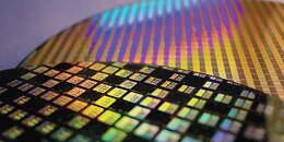
Silicon Wafer

Google to Design its Own SoCs for Pixel Smartphones and Chromebooks

Google is planning to take the Apple route in designing its own SoCs for its hardware. The company kicked off "Project Whitechapel," an initiative with technical assistance from Samsung (and possibly silicon-fabrication), to design Arm-based SoCs with specialized hardware to power Google's machine-learning tech. The first such chip will be 8-core Arm SoCs powering next-generation Pixel premium smartphones, but in the future, Google could use Arm-based SoCs to power Chromebooks.

Google has, in the past, collaborated with Intel and Qualcomm to put specialized hardware on smartphone SoCs, although the resulting chips would still be supplied by the two. "Project Whitechapel" would see Google play a dominant role in the SoC's design, with Samsung only providing technical inputs. It wouldn't be far-fetched to predict Google using lightweight variants of the SoC on its own IoT hardware, such as Chromecast and Home smart-speakers.

Samsung to Deliver 3 nm Manufacturing Process in 2022 with Next-Generation Transistors

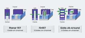
Samsung is determined in its plans to deliver the 3 nm silicon manufacturing process in the year 2022, and with it, there will be some major improvements to the transistor technology. We have already mentioned that Samsung is working on Gate-All-Around FET technology that will bring much better control of the transistor channel, preventing leakage at smaller nodes. However, today Samsung added a few more details about its upcoming Multi Bridge Channel FET technology for a 3 nm manufacturing process, simply called the MBCFET. Thanks to the report from Hardwareluxx, we have more details regarding the MBCFET technology and its characteristics.

Firstly, it is worth noting that MCBFET is a part of GAAFETs, meaning that the GAAFET is not one product, but rather a class of many based on its concepts. As far as the MCBFET performance goes, Samsung says that the technology will use 50% less power while delivering 30% more performance. There is going to be a big density gain as well, where Samsung predicts there will be around 45% less silicon space taken per one transistor. The comparison is made to an unspecified 7 nm process, possibly Samsung's process that uses FinFETs. The technology allows the stacking of transistors on top of each other, which makes it use inherently less space compared to regular FinFET. Being that MCBFET GAA transistors make its transistor width flexible, it means that the overall stacked transistor can be as wide as a designer needs it to be, adjusting for any scenario like low-power or high-performance.
Samsung GAA Samsung MBCFET

Samsung to Continue Buying LCD Screens from Sharp

It was only recently that we reported on Samsung's decision to stop manufacturing all the LCD panels and focus on the production of AMOLED and QLED displays. However, it seems like Samsung will not be abandoning the LCD technology completely. According to a report from DigiTimes, we have information that Samsung will continue to offer LCD-based screens, TN-film, various kinds of VA, IPS, etc., by buying the LCD screen from a Japanese multinational company called Sharp. Sharp will be Samsung's only source of these LCD screens, so Samsung will still be able to offer products based on them. It is reported that types of panels in question are meant for the production of television devices, meaning that they are probably bigger-sized panels.
Samsung Display

Samsung Announces Galaxy Chromebook Convertible: A "Project Athena" Chromebook

Samsung today announced the Galaxy Chromebook, a premium Google ChromeOS 2-in-1 device that converts between a conventional notebook and a tablet with a stylus. This is the first time Samsung is bringing its Android-focused Galaxy brand over to its Chromebook family. The $999 price-tag may look like a tall ask for a Chromebook, until you look at some of its specs. The star attraction is the 13.3-inch AMOLED touchscreen with 4K UHD resolution. Samsung developed the Galaxy Chromebook in close coordination with Intel as part of its ambitious "Project Athena" initiative of developing next-generation portable computing devices that defy conventions on performance and battery-life.

Under the hood is an Intel Core i5-10210U "Comet Lake" processor with 8 GB of LPDDR3-2133 memory, a 256 GB NVMe SSD, UFS + microSDXC card slot, and 802.11ax + Bluetooth connectivity (at this price we'd have expected at least 4G cellular modem). It dumps type-A USB ports and instead features a couple of type-C ports, one of which doubles up as a power input. The 4K UHD display is pulled by integrated Intel UHD 630 graphics. A 47.9 Wh battery powers the thing, with Samsung claiming 8h 20m of run-time. Measuring 30 cm x 20.32 cm x 0.99 cm (closed), the Galaxy Chromebook weighs 1.03 kg. The included S-Pen stylus slots into the body. The Galaxy Chromebook is available in two color options, red and gray, both priced at $999.
Samsung Galaxy Chromebook

Samsung 3 nm Volume Production Facing Delays in Wake of Coronavirus Impact

Samsung's 3 nm manufacturing has already given fruits to the company, with the South Korean giant already achieving risk production at the start of this year. The company previously projected volume production of their 3 nm process to start in early 2021. However, in a report via DigiTimes, this goal may have slipped to 2022 in wake of the coronavirus pandemic.

According to the news outlet, industry sources point this delay not to Samsung's fault in the manufacturing process, but to the entire logistics movement that has to be conducted in ramping up production of a new node. Impacts on logistics and transportation services are causing delays to deliveries of EUV and other critical production equipment, without which Samsung will be hard pressed to achieve its volume production goal. How this will ultimately affect Samsung's bottom line and revenue projections remains to be seen, but this won't do any favors to the company's high-density fabrication tech - especially if rival TSMC somehow manages to skirt these issues.

Samsung to End LCD Manufacturing by Late-2020, Focus on AMOLED and QLED

Samsung Display, a subsidiary of Samsung Electronics that develops and manufactures display panels, is reportedly ending the manufacturing of all its LCD panel products by the end of 2020. These include TN-film, various kinds of VA, and IPS. This would see an end to even LED-backlit LCD panels that make up a bulk of the company's low-cost PC monitors and TVs. The company will focus on more advanced panel technologies, such as AMOLED and QLED. Samsung manufactures LCD panels at plants in South Korea and China. With LCD being phased out, the production lines will be re-tooled to manufacture quantum-dot LED (QLED) panels. The company will spend the rest of 2020 shipping out pending orders of LCD panels.

U.S. Government Tightens Screws on Huawei's Global Chip Supply from TSMC

The U.S. government announced advanced measures that make it harder for foreign companies, such as Taiwan's TSMC, to supply chips to Chinese telecom hardware giant Huawei. Foreign companies that use American chipmaking equipment, are required to obtain a license from the U.S. before supplying certain chips to Huawei. Sources comment that the new rule was tailor-made to curb TSMC fabricating smartphone SoCs for Huawei's HiSilicon subsidiary.

Mainland Chinese semiconductor companies are still behind Samsung and TSMC in 7 nm-class fab technologies, forcing HiSilicon to source from the latter. 7 nm fabrication is a key requirement for SoCs and modem chips capable of 5G. The high data transceiving rates of 5G requires a certain amount of compute power that can fit into smartphone-level power-envelopes only with the help of 7 nm, at least for premium smartphone form-factors. Same applies to 5G infrastructure equipment. This is hence perceived as a means for the U.S. to clamp brakes on Huawei's plans of playing a big role in 5G tech rollouts around the world, buying western 5G tech suppliers such as Nokia time to catch up. Huawei has been a flashpoint for a bitter political spat between the U.S. and China, with the Chinese press even threatening that the matter could hamper medical supplies to the U.S. to fight the COVID-19 pandemic.

Micron to Launch HBM2 Memory This Year

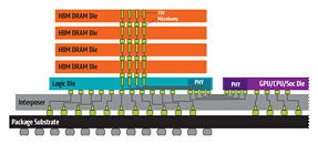
Micron Technologies, in the latest earnings report, announced that they will start shipping High-Bandwidth Memory 2 (HBM2) DRAM. Used for high-performance graphics cards, server processors and all kinds of processors, HBM2 memory is wanted and relatively expensive solution, however, when Micron enters the market of its manufacturing, prices, and the market should adjust for the new player. Previously, only SK-Hynix and Samsung were manufacturing the HBM2 DRAM, however, Micron will join them and they will again form a "big-three" pact that dominates the memory market.

Up until now, Micron used to lay all hopes on its proprietary Hybrid Memory Cube (HMC) DRAM type, which didn't gain much traction from customers and it never really took off. Only a few rare products used it, as Fujitsu SPARC64 XIfx CPU used in Fujitsu PRIMEHPC FX100 supercomputer introduced in 2015. Micron announced to suspend works on HMC in 2018 and decided to devote their efforts to GDDR6 and HBM development. So, as a result, we are seeing that they will launch HBM2 DRAM products sometime this year.
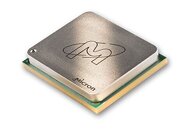
Micron HMC High-Bandwidth Memory

Samsung Announces Industry's First EUV DRAM with Shipment of First Million Modules

Samsung Electronics Co., Ltd., the world leader in advanced memory technology, today announced that it has successfully shipped one million of the industry's first 10 nm-class (D1x) DDR4 (Double Date Rate 4) DRAM modules based on extreme ultraviolet (EUV) technology. The new EUV-based DRAM modules have completed global customer evaluations, and will open the door to more cutting-edge EUV process nodes for use in premium PC, mobile, enterprise server and datacenter applications.

"With the production of our new EUV-based DRAM, we are demonstrating our full commitment toward providing revolutionary DRAM solutions in support of our global IT customers," said Jung-bae Lee, executive vice president of DRAM Product & Technology at Samsung Electronics. "This major advancement underscores how we will continue contributing to global IT innovation through timely development of leading-edge process technologies and next-generation memory products for the premium memory market."
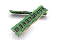
Samsung EUV DDR4

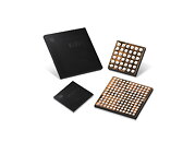
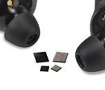
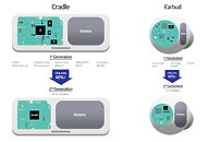
Samsung Introduces Industry's First All-in-One Power ICs Optimized for Wireless Earbuds

Samsung Electronics, a world leader in advanced semiconductor technology, today announced the industry's first all-in-one power management integrated circuits (PMIC), MUA01 and MUB01, optimized for today's True Wireless Stereo (TWS) devices.

Unlike wireless headphones, TWS earbuds have no wire that connects the two earpieces. Without the connecting wires, TWS devices present users with more freedom in movement and range on their day-to-day activities. However, like other mobile devices, long battery life and small form factors are key requirements for these wireless earbuds.
Samsung PMIC Samsung PMIC Samsung PMIC
Return to Keyword Browsing
Nov 25th, 2024 10:21 EST change timezone

New Forum Posts

Popular Reviews

Controversial News Posts