News Posts matching #Samsung

Return to Keyword Browsing

Xilinx Partners with Samsung to Develop SmartSSD CSD

Xilinx, Inc. and Samsung Electronics Co., Ltd. today announced the availability of the Samsung SmartSSD Computational Storage Drive (CSD). Powered by Xilinx FPGAs, the SmartSSD CSD is the industry's first adaptable computational storage platform providing the performance, customization, and scalability required by data-intensive applications.

Xilinx will showcase the SmartSSD CSD and partner solutions at the Flash Memory Summit Virtual Conference and Expo taking place November 10-12. The SmartSSD CSD is a flexible, programmable storage platform that developers can use to create a variety of unique and scalable accelerators that solve a broad range of data center problems. It empowers a new breed of software developers to easily build innovative hardware-accelerated solutions in familiar high-level languages. The SmartSSD CSD accelerates data processing performance by 10x or more for applications such as database management, video processing, artificial intelligence layers, complex search, and virtualization.

Samsung Could Become Apple's Newest Chip Supplier

Apple has recently announced its transition to Apple Silicon, meaning that every processor inside its products will be custom designed by the company. However, that seems to be becoming a bit of a problem. The sole supplier of chips for Apple has been Taiwan Semiconductor Manufacturing Company (TSMC), which Apple collaborated with for the past few years. The sheer capacity of TSMC is enough to satisfy the demand from several companies and thus it allows some of them to book its capacity. With Apple demanding more and more capacity than ever before, it is becoming quite hard to keep up with it. That is why Apple is, according to some analysts for Business Korea, looking for a foundry beyond TSMC's to manufacture its chips.

According to the source, Apple is looking at the direction of Samsung Electronics and its silicon manufacturing facilities. Samsung has recently started the production of its 5 nm silicon manufacturing node. We have reported that the first SoCs are set to arrive soon. However, it may be possible that Apple's M1 lineup of SoCs will be a part of that first wave. Apple is reportedly going to tap both TSMC and Samsung to qualify enough supply for the huge demand of the products based on the latest 5 nm technology.

Samsung's 5 nm Node in Production, First SoCs to Arrive Soon

During its Q3 earnings call, Samsung Electronics has provided everyone with an update on its foundry and node production development. In the past year or so, Samsung's foundry has been a producer of a 7 nm LPP (Low Power Performance) node as its smallest node. That is now changed as Samsung has started the production of the 5 nm LPE (Low Power Early) semiconductor manufacturing node. In the past, we have reported that the company struggled with yields of its 5 nm process, however, that seems to be ironed out and now the node is in full production. To contribute to the statement that the new node is doing well, we also recently reported that Samsung will be the sole manufacturer of Qualcomm Snapdragon 875 5G SoC.

The new 5 nm semiconductor node is a marginal improvement over the past 7 nm node. It features a 10% performance improvement that is taking the same power and chip complexity or a 20% power reduction of the same processor clocks and design. When it comes to density, the company advertises the node with x1.33 times increase in transistor density compared to the previous node. The 5LPE node is manufactured using the Extreme Ultra-Violet (EUV) methodology and its FinFET transistors feature new characteristics like Smart Difusion Break isolation, flexible contact placement, and single-fin devices for low power applications. The node is design-rule compatible with the previous 7 nm LPP node, so the existing IP can be used and manufactured on this new process. That means that this is not a brand new process but rather an enhancement. First products are set to arrive with the next generation of smartphone SoCs, like the aforementioned Qualcomm Snapdragon 875.

G.Skill Announces Extreme Low Latency DDR4-3600 CL14 64GB Memory Kit

G.SKILL International Enterprise Co., Ltd., the world's leading manufacturer of extreme performance memory and gaming peripherals, is delighted to announce extreme low-latency with high-capacity DDR4 memory kits at DDR4-3600 CL14-15-15-35 in 64 GB (16GBx4) and 32 GB (16GBx2) configurations under the Trident Z Neo, Trident Z Royal, Trident Z RGB, and Ripjaws V series. Once again, these extraordinary memory kits are manufactured using high-performance Samsung B-die ICs to achieve the low latency of CL14 at DDR4-3600.

At G.SKILL, we are always searching for the ultimate memory kit, tuned not only for speed, but also for efficiency. And to achieve high efficiency, this means lower latency timings. As the market demand for higher capacity increases, G.SKILL has risen to the challenge, and is introducing the DDR4-3600 CL14-15-15-35 64 GB (16 GB x4) memory kit specification, shown validated on the Intel-based ASUS ROG MAXIMUS XII HERO (WI-FI) Z490 and MSI MEG Z490 GODLIKE motherboards, as well as the AMD-based ASUS PRIME X570-P motherboard.

Raja Koduri to Present at Samsung Foundry Forum amid Intel's Outsourcing Efforts

Intel's chief architect and senior vice president of discrete graphics division, Mr. Raja Koduri, is said to be scheduled to present at Samsung Electronics Event day. With a presentation titled "1000X More Compute for AI by 2025", the event is called Samsung Foundry SAFE Forum. It is a global virtual conference designed to be available to everyone. So you might be wondering what is Mr. Koduri doing there. Unless you have been living under a rock, you know about Intel's struggles with node manufacturing. Specifically, the 10 nm node delays that show the company's efforts to deliver a node on time. The same is happening with the 7 nm node that also experienced significant delays.

Intel has a contract to develop an exascale supercomputer at Argonne National Laboratory, called Aurora. That supercomputer is using Intel's CPUs and the company's upcoming Xe GPUs. Since the company has problems with manufacturing and has to deliver the products (it is bound by several contracts) to its contractors and customers, it decided to look at external manufacturers for its products, specifically Xe graphics. Being that Mr. Koduri tweeted an image of him visiting Samsung Giheung Fab in Korea, and now presenting at the Samsung Foundry event, it is possible that Intel will tap Samsung's semiconductor manufacturing process for its Xe GPU efforts and that Samsung will be the contractor in charge.

AMD Radeon RX 6000 Series "Big Navi" GPU Features 320 W TGP, 16 Gbps GDDR6 Memory

AMD is preparing to launch its Radeon RX 6000 series of graphics cards codenamed "Big Navi", and it seems like we are getting more and more leaks about the upcoming cards. Set for October 28th launch, the Big Navi GPU is based on Navi 21 revision, which comes in two variants. Thanks to the sources over at Igor's Lab, Igor Wallossek has published a handful of information regarding the upcoming graphics cards release. More specifically, there are more details about the Total Graphics Power (TGP) of the cards and how it is used across the board (pun intended). To clarify, TDP (Thermal Design Power) is a measurement only used to the chip, or die of the GPU and how much thermal headroom it has, it doesn't measure the whole GPU power as there are more heat-producing components.

So the break down of the Navi 21 XT graphics card goes as follows: 235 Watts for the GPU alone, 20 Watts for Samsung's 16 Gbps GDDR6 memory, 35 Watts for voltage regulation (MOSFETs, Inductors, Caps), 15 Watts for Fans and other stuff, and 15 Watts that are used up by PCB and the losses found there. This puts the combined TGP to 320 Watts, showing just how much power is used by the non-GPU element. For custom OC AIB cards, the TGP is boosted to 355 Watts, as the GPU alone is using 270 Watts. When it comes to the Navi 21 XL GPU variant, the cards based on it are using 290 Watts of TGP, as the GPU sees a reduction to 203 Watts, and GDDR6 memory uses 17 Watts. The non-GPU components found on the board use the same amount of power.

NVIDIA Reportedly Moving Ampere to 7 nm TSMC in 2021

A report straight from DigiTimes claims that NVIDIA is looking to upgrade their Ampere consumer GPUs from Samsung's 8 nm to TSMC's 7 nm. According to the source, the volume of this transition should be "very large", but most likely wouldn't reflect the entirety of Ampere's consumer-facing product stack. The report claims that TSMC has become more "friendly" to NVIDIA. This could be because TSMC now has available manufacturing capacity in 7 nm due to some of its clients moving to the company's 5 nm node, or simply because TSMC hadn't believed NVIDIA to consider Samsung as a viable foundry alternative - which it now does - and has thus lowered pricing.

There are various reasons being leveraged at this, none with substantial grounds other than "reported from industry sources". NVIDIA looking for better yields is one of the appointed reasons, as is its history as a TSMC customer. NVIDIA shouldn't have too high a cost porting its manufacturing to TSMC in terms of design changes to the silicon level so as to cater to different characteristics of TSMC's 7 nm, because the company's GA100 GPU (Ampere for the non-consumer market) is already manufactured at TSMC. The next part of this post is mere (relatively informed) speculation, so take that with a saltier disposition than what came before.

TSMC Begins Construction of 2 nm Manufacturing Facility

TSMC, the leading semiconductor foundry in the world, has reportedly begun construction of its 2 nm manufacturing facility. According to a DigiTimes report, translated by @chiakokhua on Twitter, besides the construction of 2 nm R&D center, TSMC has also started the construction of the manufacturing facility for that node, so it will be ready in time. Please do note that the node name doesn't represent the size of the transistor, so it will not actually be 2 nm wide. The new facilities will be located near TSMC's headquarters in Hsinchu Science Park, Taiwan. The report also confirms the first details about the node, specifically that it will use Gate-All-Around (GAA) technology. And there is also another interesting piece of information regarding even smaller node, the planning for 1 nm node has begun according to the source.

Besides advanced nodes, TSMC also laid out clear plans to accelerate the push of advanced packaging technology. That includes SoIC, InFO, CoWoS, and WoW. All of these technologies are classified as "3D Fabric" by the company, even though some are 2.5D. These technologies will be mass-produced at "ZhuNan" and "NanKe" facilities starting in the second half of 2021, and are expected to significantly contribute to the company's profits. It is also reported that the competing foundry, Samsung, has a 3D packaging technology of its own called X-cube, however, it is attracting customers a lot slower than TSMC due to the high costs of the new technology.

Samsung Delivers Next-Level SSD Performance with 980 PRO

Samsung Electronics, the world leader in advanced memory technology, today unveiled the company's first consumer PCIe 4.0 NVMe solid state drive (SSD) - the Samsung SSD 980 PRO. The new 980 PRO is designed for professionals and consumers who want cutting-edge performance in their high-end PCs, workstations and game consoles.

"Over the years, Samsung has continuously challenged the limits of high-speed flash memory storage solutions," said Dr. Mike Mang, vice president of Memory Brand Product Biz at Samsung Electronics. "The new 980 PRO SSD reflects our continuing commitment to delivering exceptional products consumers have come to expect from Samsung."

Samsung Foundry to Become Sole Manufacturer of Qualcomm Snapdragon 875 on 5 nm EUV Manufacturing Process

Rumors fresh of South Korean shores claim that Samsung has snagged a position as sole provider for Qualcomm's Snapdragon 875 SoC on its 5 nm EUV manufacturing process. The reason for this, according to a supposed industry insider, boiled down to money (as it almost always does): Samsung simply offered lower pricing for chips manufactured under its 5 nm EUV process than TSMC did. The deal has been claimed to be worth some $840M. This makes sense, as Samsung has a considerable product portfolio - including lucrative memory fabrication - from which it can pool resources so as to lower pricing for new manufacturing technologies, whereas TSMC can only count on revenues it brings in from contracted silicon manufacturing deals.

Samsung's 5 nm EUV will still offer the now tried-and-true FinFet transistor design - next-generation GAAFET (gate all-around FET) are reserved for the companies' 3 nm efforts. This piece of news directly contradicts Digitimes' earlier reporting on Qualcomm leaving Samsung as a foundry partner due to lower than adequate yields for Samsung's 5 nm EUV. With Samsung already manufacturing NVIDIA's Ampere on its 8 nm node, and now with a confirmed high-volume client with Qualcomm, this likely means more available capacity for other TSMC clients - of which we could mention AMD and Apple.

NVIDIA GeForce RTX Ampere Chips Feature Three Binning Tiers, Mostly Good Dies are Present

Chip binning is a process of sorting out the manufactured silicon by quality. That means that each chip that comes from the silicon wafer is tested and sorted by different features. For example, a chip is tested for how much voltage it takes for operation, how cool it runs, and of course how it overclocks. By putting their chips through various testing, manufacturers often create binning tiers, where they can differentiate good and bad chips, so they know where to send, and if they should send the chips. The biggest and most complex approach for sending chips is for graphics cards. As there are different AIBs, manufacturers like NVIDIA and AMD need to send them chips of various qualities to incorporate in their products. It is a rather time-consuming and complex process to find out the bin type and the tier of chips, however today we are getting some information from Igor's Lab.

According to their sources, it is said that NVIDIA's latest GeForce RTX Ampere lineup features three binning tiers. There is "Bin 0" which represents an okay chip that can perform as intended, "Bin 1" chips which are good processors, and "Bin 2" processors which represent the best quality chips with the highest performance characteristics. These "Bin 2" dies run cooler compared to the rest and achieve higher overclocking speed. In reality, the binning represents coordination between the chip designer (NVIDIA in this case) and the manufacturer (Samsung with its 8N 8 nm process). It is said that from the complete pilot run of Ampere chips, Samsung ends up with 30% of the "Bin 0" dies, 60% of "Bin 1" dies, and only 10% of "Bin 2" dies. The production period was quite short and these numbers are good for Samsung, as they probably didn't have much time to work on it, so we can expect these numbers to improve.

Alleged AMD Radeon "Big Navi" Prototype Pictured

Following Wednesday's announcement of the Radeon RX 6000 series with product launches on October 28, the rumor mill started rolling full steam ahead. The RX 6000 series GPUs by AMD will be based on the RDNA2 graphics architecture, the same exact architecture powering the Xbox Series X and PlayStation 5, and will feature DirectX 12 Ultimate support, including hardware raytracing. A PC enthusiast on Chinese microblogging site Bilibili posted a picture of an alleged "Big Navi" prototype. Since its July 2019 debut, there have been rumors of AMD working on a new high-end GPU to take on the upper-segment of NVIDIA, given that the RX 5700 series offered competitive performance to NVIDIA's breadwinning products, such as the RTX 2070 series and RTX 2060 series.

The picture reveals the reverse side of the alleged "Big Navi" prototype's PCB, showing a larger cluster of GPU ancillaries than those behind a "Navi 10," and eight memory pads with the paper labels "Typical XT ASIC" references for a "16 Gb Samsung GDDR6 memory." Over a 256-bit wide memory interface, the chip should hence have 16 GB of GDDR6 memory. Since this is a prototype, several headers are sticking out of the PCB for the design and prototyping of the product. A tower-type CPU cooler has been MacGyvered onto the GPU (which isn't uncommon for VGA prototypes). We'll hear a lot more about this product in the run up to its October 28 launch.

Samsung and SK Hynix to Impose Sanctions Against Huawei

Ever since the Trump administration imposed sanctions against Huawei to stop it from purchasing parts from third-party vendors to bypass the ban announced back in May, some vendors continued to supply the company. So it seems like some Korean manufacturers will be joining the doings of the US government, and apply restrictions to Huawei. According to the reports of South Korean media outlets, Samsung Electronics and SK Hynix will be joining the efforts of the US government and the Trump administration to impose sanctions against Chinese technology giant - Huawei.

It is reported that on September 15th, both Samsung and SK Hynix will stop any shipments to Huawei, where Samsung already stopped efforts for creating any new shipments. SK Hynix is said to continue shipping DRAM and NAND Flash products until September 14th, a day before the new sanctions are applied. Until the 14th, Huawei will receive some additional chips from SK Hynix. And it is exactly SK Hynix who is said to be a big loser here. It is estimated that 41.2% of SK Hynix's H1 2020 revenue came from China, most of which was memory purchased for Huawei phones and tablets. If the company loses Huawei as a customer, it would mean that the revenue numbers will be notably lower.

NVIDIA Announces GeForce Ampere RTX 3000 Series Graphics Cards: Over 10000 CUDA Cores

NVIDIA just announced its new generation GeForce "Ampere" graphics card series. The company is taking a top-to-down approach with this generation, much like "Turing," by launching its two top-end products, the GeForce RTX 3090 24 GB, and the GeForce RTX 3080 10 GB graphics cards. Both cards are based on the 8 nm "GA102" silicon. Join us as we live blog the pre-recorded stream by NVIDIA, hosted by CEO Jen-Hsun Huang.

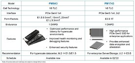
Samsung 980 PRO NVMe SSD Uses TLC NAND Flash with Half the Endurance of 970 PRO: Product Page

Samsung's hotly anticipated 980 PRO M.2 NVMe flagship client-segment SSD is the company's first "PRO" branded SSD to feature TLC NAND flash memory, breaking from a unique tradition of using MLC (2 bits per cell) NAND flash. Product pages of the drive went live, and its specifications clearly state the use of "Samsung V-NAND 3-bit MLC," which is another way of saying TLC. "MLC" generally referred to as NAND flash memory that stores 2 bits per cell, even through the term "Multi-level" is amorphous.

The product page lists other juicy specs of Samsung's first M.2 NVMe client SSD that takes advantage of PCI-Express gen 4. The drive uses Samsung's in-house design "Elpis" controller, which uses NVMe 1.3 protocol over PCI-Express 4.0 x4, and an LPDDR4 DRAM cache. The 980 PRO comes in capacities of up to 1 TB, with up to 1 GB of DRAM cache. Samsung rates the 1 TB version as capable of up to 7000 MB/s sequential reads, up to 5000 MB/s sequential writes, and up to 1 million IOPS 4K random reads/writes at QD32. The use of TLC impacts endurance adversely in comparison to that of the drive's immediate predecessor, the 970 PRO, with the 1 TB 980 PRO warranty covering only up to 600 TBW, in comparison to 1200 TBW of the 970 PRO 1 TB, and the 500 GB 980 PRO offering just 300 TBW warranty coverage in comparison to 600 TBW of the 970 PRO 512 GB.

Samsung Begins Mass Production of 16Gb LPDDR5 DRAM at World's Largest Semiconductor Line

Samsung Electronics, the world leader in advanced memory technology, today announced that its second production line in Pyeongtaek, Korea, has commenced mass production of the industry's first 16-gigabit (Gb) LPDDR5 mobile DRAM, using extreme ultraviolet (EUV) technology. Built on Samsung's third-generation 10 nm-class (1z) process, the new 16Gb LPDDR5 boasts the highest mobile memory performance and largest capacity to enable more consumers to enjoy the full benefits of 5G and AI features in next-generation smartphones.

"The 1z-based 16Gb LPDDR5 elevates the industry to a new threshold, overcoming a major developmental hurdle in DRAM scaling at advanced nodes," said Jung-bae Lee, executive vice president of DRAM Product & Technology at Samsung Electronics. "We will continue to expand our premium DRAM lineup and exceed customer demands, as we lead in growing the overall memory market."

TSMC Owns 50% of All EUV Machines and Has 60% of All EUV Wafer Capacity

TSMC had been working super hard in the past few years and has been investing in lots of new technologies to drive the innovation forward. At TSMC's Technology Symposium held this week was, the company has presented various things like the update on its 12 nm node, as well as future plans for node development. One of the most interesting announcements made this week was TSMC's state and ownership of Extreme Ultra-Violet (EUV) machines. ASML, the maker of these EUV machines used to etch the pattern on silicon, has been the supplier of the Taiwanese company. TSMC has announced that they own an amazing 50% of all EUV machine installations.

What is more important is the capacity that the company achieves with it. It is reported that TSMC achieves 60% of all EUV wafer capacity in the world, which is a massive achievement of what TSMC can do with the equipment. The company right now has only two nodes on EUV in high-volume manufacturing, the 7 nm+ node and 5 nm node (which is going HVM in Q4), however, that is more than any of its competitors. All of the future nodes are to be manufactured using the EUV machines and the smaller nodes require it. As far as the competitors go, only Samsung is currently making EUV silicon on the 7 nm LPP node. Intel is yet to release some products on a 7 nm node of its own, which is the first EUV node from the company.

NAND Flash Revenue Rises 6.5% QoQ in 2Q20 Due to Pandemic-Induced Demand Growth for Cloud Services, Says TrendForce

The NAND Flash industry benefitted from strong demand for PCs and servers in 2Q20 as the COVID-19 pandemic caused a demand surge for cloud services and technologies that are related to working from home, according to TrendForce's latest investigations. This, in turn, kept demand high for SSDs. However, the smartphone and consumer electronics markets had not recovered from the impact of the pandemic. The demand for these products therefore declined compared to the previous quarter. In 2Q20, total NAND Flash bit shipment and ASP both experienced a minor increase of about 3% QoQ, while NAND Flash revenue reached US$14.5 billion, a 6.5% increase QoQ.

DRAM Revenue Rises by 15.4% in 2Q20, with Possible Decline in Prices Expected for 3Q20, Says TrendForce

The last cyclical upturn in DRAM contract prices began at the start of 2020 and was led by server DRAM, according to TrendForce's latest investigations. In 2Q20, the emergence of the COVID-19 pandemic shocked the global economy, but OEMs maintained or even stepped up procurement of components because they feared disruptions in the supply chain. As a result, DRAM suppliers' bit shipments surpassed expectations for the quarter, in turn widening the overall increase in DRAM ASP and raising the global DRAM revenue by 15.4% QoQ in 2Q20 to US$17.1 billion.

Nevertheless, TrendForce indicates that server OEMs are now carrying a rather high level of DRAM inventory after aggressively stocking up for two consecutive quarters. At the same time, customers of enterprise servers are holding back on procurement because the economic outlook is getting bleaker and more uncertain. Since server DRAM has the unique role of leading cyclical changes, this category is going to be first to experience price drop in the next downturn and thereby pull prices down for other types of DRAM products. As such, TrendForce forecasts at best a flattening of product shipments and decrease in DRAM prices in 3Q20, with DRAM suppliers suffering a decline in profitability.

DigiTimes Research: Korean Memory Makers See Output Value Surge in Q2

According to the latest DigiTimes Research report, it is said that Korean memory makers have experienced a surge in chip output value. Korean memory manufacturers are Samsung Electronics and SK Hynix, which both have seen a massive growth of 22.1% on a yearly basis and 13.9% sequentially in the second quarter of 2020. This is no small feat as the demand for memory in the smartphone industry has been slowed in that period due to the COVID pandemic, however, it was offset by strong demand from servers and notebooks. When the output of Korean memory giants is fused, Samsung and SK Hynix had combined revenue of KRW22.9 trillion or about 20.8 billion USD. The demand for memory is expected to continue its growth due to the 5G headset market.

Samsung and Logitech Announce Strategic Partnership

As people around the world increasingly demand convenient and efficient collaboration technology, the time has come for major industry players to combine their expertise and create solutions that allow users to get the best experience, no matter where they are.

The video conferencing market is set to reach a revenue of $50 billion (USD) by 2026, from having only reached $14 billion in 2019. This dramatic acceleration in the market is due to the current global climate, which has shifted the way businesses behave and operate. As such, video conferencing has quickly become an important platform for communicating and ensuring business continuity. In fact, global weekly downloads of business apps surged from 33.7 million in early October 2019 to 80 million in mid-April 2020. Video conferencing app downloads have also increased from five million a week to 50 million in the same period.

Samsung Aims to Become Number One Android AP Vendor by Joining Forces with AMD and Arm

Samsung Electronics has reportedly laid out a plan to become the number one Android application processor (AP) vendor in the industry with its plan to join forces with AMD and Arm. The report of Business Korea indicates that Samsung wants to use both company's knowledge and IP to produce the best possible silicon. In early November of last year, Samsung has decided to shut down its division responsible for making custom CPU designs, and to start licensing IP from Arm. Also last year, Samsung has announced a strategic partnership with AMD to use its RDNA graphics processors in smartphones.

So Samsung plans to license IPs from both companies and just put them in SoC that will be up to the task to deliver the best performance, as the company predicts. The CPU is reportedly going to be based on Arm's Cortex-X custom design that should deliver high-performance Samsung wants. In the past, the company had some problems with the heat-management of its CPUs as they were designed a bit inefficiently. To cover everything, Samsung also plans to increase the number of employees working on a neural processing unit (NPU) and make a good performing NPUs as well, to combine with the rest of IPs.

Samsung Announces Availability of its Silicon-Proven 3D IC Technology

Samsung Electronics Co., Ltd., a world leader in advanced semiconductor technology, today announced the immediate availability of its silicon-proven 3D IC packaging technology, eXtended-Cube (X-Cube), for today's most advanced process nodes. Leveraging Samsung's through-silicon via (TSV) technology, X-Cube enables significant leaps in speed and power efficiency to help address the rigorous performance demands of next-generation applications including 5G, artificial intelligence, high-performance computing, as well as mobile and wearable.

"Samsung's new 3D integration technology ensures reliable TSV interconnections even at the cutting-edge EUV process nodes," said Moonsoo Kang, senior vice president of Foundry Market Strategy at Samsung Electronics. "We are committed to bringing more 3D IC innovation that can push the boundaries of semiconductors."

Samsung Display Commercializes New Variable Refresh Rate Tech for Mobile Device Power Saving

Samsung Display Company today revealed new display technology that features a remarkable power-saving function for mobile electronics, being commercialized for the first time in Galaxy Note 20 Ultra 5G flagship smartphones. The display company has now successfully commercialized its low-power OLED adaptive frequency technology, which can curtail the operating power of a phone's display by as much as 22 percent over existing smartphones now in general use.

"High-definition video streaming and gaming are expanding their capabilities in line with 5G commercialization, creating a widespread need for display panel technologies that can enable greater power savings," said Ho-Jung Lee, Vice President of the mobile display product planning team for Samsung Display. "Our Adaptive Frequency display technology is expected to considerably enhance the user experience by calibrating refresh rates in line with the requirements of a specific application and therein more precisely allocating available power. This will free up time for other smartphone operations," Lee added.

Softbank Approaches TSMC and Foxconn for Potential Arm Buyout

Softbank-owned company Arm Ltd. has been a subject to a round of rumors regarding the potential buyout of the company because Softbank has considered selling it for some time. The company has approached NVIDIA, with their talks getting "advanced", and Samsung wants a piece of the cake as well. It is now reported that Softbank has approached TSMC and Foxconn as well, regarding a potential Arm takeover. In the report by Nikkei Asia, we have found out that Arm has shared the same financial data points and business plan with TSMC and Foxconn, the same way company did with NVIDIA.
If TSMC and Foxconn have any interest in the company, it would be necessary to create a consortium that would operate Arm Ltd. With NVIDIA, Samsung, and these two new players, the consortium would already count four companies. Nikkei sources claim that Apple and Qualcomm have been also included in the poll of potential buyers, which would make the idea of establishing a consortium very valid.
Return to Keyword Browsing
Nov 25th, 2024 10:49 EST change timezone

New Forum Posts

Popular Reviews

Controversial News Posts