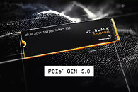
Sandisk Launches WD_BLACK SN8100 PCIe Gen 5.0 NVMe SSD
Setting a new standard for client SSDs, Sandisk today unveiled the powerful WD_BLACK SN8100 NVMe SSD with PCIe Gen 5.0 technology, a cutting-edge internal SSD delivering speeds up to 14,900 MB/s and capacities up to 8 TB, for high-performance gaming, content creation and artificial intelligence (AI) workloads.
With the evolution of gaming graphics, high-quality 4K and 8K content and AI applications, today's gamers and professionals need solutions to help maximize the performance of their PCs. The Sandisk WD_BLACK SN8100 NVMe PCIe Gen 5.0 SSD is built for hardcore PC gamers looking to add the most advanced combination of speed and reliability to their rig for peak performance and for professionals needing a top-of-the-line PC storage solution for intensive workflows and AI applications. In addition to blistering speeds, the new PCIe Gen 5.0 SSD is also 100% more power efficient than Sandisk's high-performance PCIe Gen 4.0 SSD.
With the evolution of gaming graphics, high-quality 4K and 8K content and AI applications, today's gamers and professionals need solutions to help maximize the performance of their PCs. The Sandisk WD_BLACK SN8100 NVMe PCIe Gen 5.0 SSD is built for hardcore PC gamers looking to add the most advanced combination of speed and reliability to their rig for peak performance and for professionals needing a top-of-the-line PC storage solution for intensive workflows and AI applications. In addition to blistering speeds, the new PCIe Gen 5.0 SSD is also 100% more power efficient than Sandisk's high-performance PCIe Gen 4.0 SSD.


