News Posts matching #SoC

Return to Keyword Browsing

U.S. Government Tightens Screws on Huawei's Global Chip Supply from TSMC

The U.S. government announced advanced measures that make it harder for foreign companies, such as Taiwan's TSMC, to supply chips to Chinese telecom hardware giant Huawei. Foreign companies that use American chipmaking equipment, are required to obtain a license from the U.S. before supplying certain chips to Huawei. Sources comment that the new rule was tailor-made to curb TSMC fabricating smartphone SoCs for Huawei's HiSilicon subsidiary.

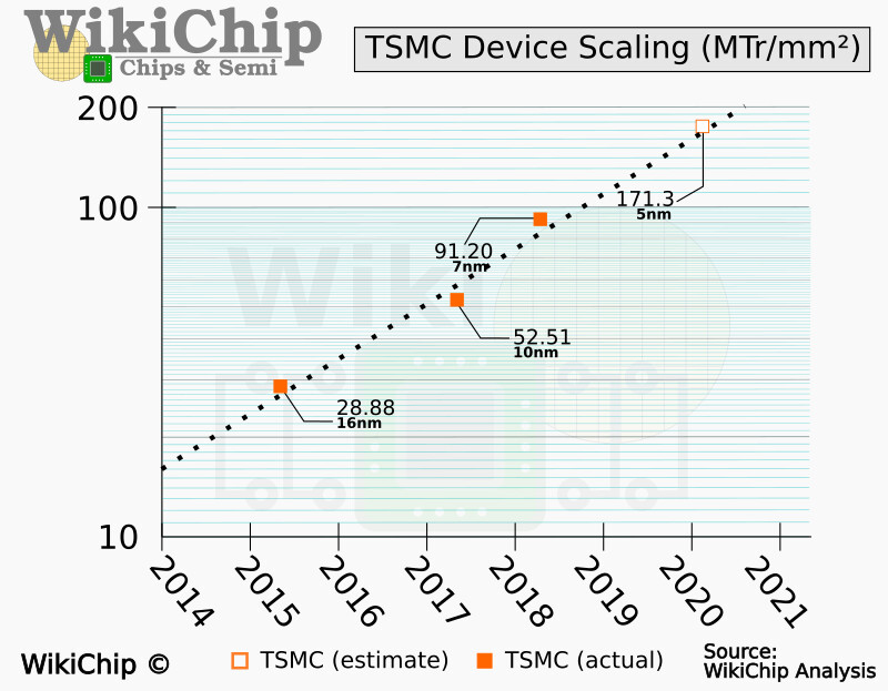
Mainland Chinese semiconductor companies are still behind Samsung and TSMC in 7 nm-class fab technologies, forcing HiSilicon to source from the latter. 7 nm fabrication is a key requirement for SoCs and modem chips capable of 5G. The high data transceiving rates of 5G requires a certain amount of compute power that can fit into smartphone-level power-envelopes only with the help of 7 nm, at least for premium smartphone form-factors. Same applies to 5G infrastructure equipment. This is hence perceived as a means for the U.S. to clamp brakes on Huawei's plans of playing a big role in 5G tech rollouts around the world, buying western 5G tech suppliers such as Nokia time to catch up. Huawei has been a flashpoint for a bitter political spat between the U.S. and China, with the Chinese press even threatening that the matter could hamper medical supplies to the U.S. to fight the COVID-19 pandemic.

TSMC N5P 5nm Node Offers 84-87% Transistor Density Gain Over Current 7nm Node

A WikiChip analysis of TSMC's next-generation 5 nanometer N5P silicon fabrication node estimates a massive 84-87% increase in transistor densities on offer compared to the company's first commercial 7 nm-class node, the N7 (7 nm DUV). The report estimates an 87% transistor-density increase, even though TSMC's own figure is slightly modest, at 84%. TSMC N5P node is expected to commence production later this year. Its precursor, TSMC N5, began risk production earlier this year, with production on the node commencing in April or May, unless derailed by the COVID-19 pandemic. The N5P node provides transistor densities of an estimated 171.3 million transistors per mm² die area, compared to 91.2 mTr/mm² of N7. Apple is expected to be the node's biggest customer in 2020, with the company building its A14-series SoC on it.

BIOSTAR Announces the A68N-2100K SoC Motherboard

BIOSTAR, a leading brand of motherboards, graphics cards, and storage devices, today announces the A68N-2100K SoC motherboard that comes with an in-built AMD E1-6010 Processor. Throughout many decades, BIOSTAR has been revered as one of the best manufacturers of robust, highly reliable motherboards with a wide array of models on both Intel and AMD platforms to choose from and a plethora of supplementary components catering to many user preferences globally.

Modern technology meets sleek, refined form factor as BIOSTAR's A68N-2100K SoC Mini-ITX motherboard is unveiled to the world with an inbuilt AMD E1-6010 Processor and support for AMD Radeon R2 Graphics.

Sony Reveals PS5 Hardware: RDNA2 Raytracing, 16 GB GDDR6, 6 GB/s SSD, 2304 GPU Cores

Sony in a YouTube stream keynote by PlayStation 5 lead system architect Mark Cerny, detailed the upcoming entertainment system's hardware. There are three key areas where the company has invested heavily in driving forward the platform by "balancing revolutionary and evolutionary" technologies. A key design focus with PlayStation 5 is storage. Cerny elaborated on how past generations of the PlayStation guided game developers' art direction as the low bandwidths and latencies of optical discs and HDDs posed crippling latencies arising out of mechanical seeks, resulting in infinitesimally lower data transfer rates than what the media is capable of in best case scenario (seeking a block of data from its outermost sectors). SSD was the #1 most requested hardware feature by game developers during the development of PS5, and Sony responded with something special.

Each PlayStation 5 ships with a PCI-Express 4.0 x4 SSD with a flash controller that has been designed in-house by Sony. The controller features 12 flash channels, and is capable of at least 5.5 GB/s transfer speeds. When you factor in the exponential gains in access time, Sony expects the SSD to provide a 100x boost in effective storage sub-system performance, resulting in practically no load times.

Complete Hardware Specs Sheet of Xbox Series X Revealed

Microsoft just put out of the complete hardware specs-sheet of its next-generation Xbox Series X entertainment system. The list of hardware can go toe to toe with any modern gaming desktop, and even at its production scale, we're not sure if Microsoft can break-even at around $500, possibly counting on game and DLC sales to recover some of the costs and turn a profit. To begin with the semi-custom SoC at the heart of the beast, Microsoft partnered with AMD to deploy its current-generation "Zen 2" x86-64 CPU cores. Microsoft confirmed that the SoC will be built on the 7 nm "enhanced" process (very likely TSMC N7P). Its die-size is 360.45 mm².

The chip packs 8 "Zen 2" cores, with SMT enabling 16 logical processors, a humongous step up from the 8-core "Jaguar enhanced" CPU driving the Xbox One X. CPU clock speeds are somewhat vague. It points to 3.80 GHz nominal and 3.66 GHz with SMT enabled. Perhaps the console can toggle SMT somehow (possibly depending on whether a game requests it). There's no word on the CPU's cache sizes.

Researchers Find Unfixable Vulnerability Inside Intel CPUs

Researchers have found another vulnerability Inside Intel's Converged Security and Management Engine (CSME). For starters, the CSME is a tiny CPU within a CPU that has access to whole data throughput and is dedicated to the security of the whole SoC. The CSME system is a kind of a black box, given that Intel is protecting its documentation so it can stop its copying by other vendors, however, researchers have discovered a flaw in the design of CSME and are now able to exploit millions of systems based on Intel CPUs manufactured in the last five years.

Discovered by Positive Technologies, the flaw is lying inside the Read-Only Memory (ROM) of the CSME. Given that the Mask ROM is hardcoded in the CPU, the exploit can not be fixed by a simple firmware update. The researchers from Positive Technologies describe it as such: "Unfortunately, no security system is perfect. Like all security architectures, Intel's had a weakness: the boot ROM, in this case. An early-stage vulnerability in ROM enables control over the reading of the Chipset Key and generation of all other encryption keys. One of these keys is for the Integrity Control Value Blob (ICVB). With this key, attackers can forge the code of any Intel CSME firmware module in a way that authenticity checks cannot detect. This is functionally equivalent to a breach of the private key for the Intel CSME firmware digital signature, but limited to a specific platform."

UNISOC Launches Next-Gen 5G SoC T7520 on 6 nm EUV Manufacturing Node

UNISOC, a leading global supplier of mobile communication and IoT chipsets, today officially launched its new-generation 5G SoC mobile platform - T7520. Using cutting-edge process technology, T7520 enables an optimized 5G experience with substantially enhanced AI computing and multimedia imaging processing capabilities while lowering power consumption.

T7520 is UNISOC's second-generation 5G smartphone platform. Built on a 6 nm EUV process technology and empowered by some of the latest design techniques, it offers substantially enhanced performance at a lower level of power consumption than ever.

Ampere Computing Uncovers 80 Core "Cloud-Native" Arm Processor

Ampere Computing, a startup focusing on making HPC and processors from cloud applications based on Arm Instruction Set Architecture, today announced the release of a first 80 core "cloud-native" processor based on the Arm ISA. The new Ampere Altra CPU is the company's first 80 core CPU meant for hyper scalers like Amazon AWS, Microsoft Azure, and Google Cloud. Being built on TSMC's 7 nm semiconductor manufacturing process, the Altra is a CPU that is utilizing a monolithic die to achieve maximum performance. Using Arm's v8.2+ instruction set, the CPU is using the Neoverse N1 platform as its core, to be ready for any data center workload needed. It also borrows a few security features from v8.3 and v8.5, namely the hardware mitigations of speculative attacks.

When it comes to the core itself, the CPU is running at 3.0 GHz frequency and has some very interesting specifications. The design of the core is such that it is 4-wide superscalar Out of Order Execution (OoOE), which Ampere refers to as "aggressive" meaning that there is a lot of data throughput going on. The cache levels are structured in a way that there is 64 KB of L1D and L1I cache per core, along with 1 MB of L2 cache per core as well. For system-level cache, there is 32 MB of L3 available to the SoC. All of the caches have Error-correcting code (ECC) built-in, giving the CPU a much-needed feature. There are two 128-bit wide Single Instruction Multiple Data (SIMD) units, which are there to do parallel processing if needed. There is no mention if they implement Arm's Scalable Vector Extensions (SVE) or not.

TSMC and Broadcom Enhance the CoWoS Platform with World's First 2X Reticle Size Interposer

TSMC today announced it has collaborated with Broadcom on enhancing the Chip-on-Wafer-on-Substrate (CoWoS ) platform to support the industry's first and largest 2X reticle size interposer. With an area of approximately 1,700mm2, this next generation CoWoS interposer technology significantly boosts computing power for advanced HPC systems by supporting more SoCs as well as being ready to support TSMC's next-generation five-nanometer (N5) process technology.

This new generation CoWoS technology can accommodate multiple logic system-on-chip (SoC) dies, and up to 6 cubes of high-bandwidth memory (HBM), offering as much as 96 GB of memory. It also provides bandwidth of up to 2.7 terabytes per second, 2.7 times faster than TSMC's previously offered CoWoS solution in 2016. With higher memory capacity and bandwidth, this CoWoS solution is well-suited for memory-intensive workloads such as deep learning, as well as workloads for 5G networking, power-efficient datacenters, and more. In addition to offering additional area to increase compute, I/O, and HBM integration, this enhanced CoWoS technology provides greater design flexibility and yield for complex ASIC designs in advanced process nodes.

SK Hynix Licenses DBI Ultra 3D Interconnect Technology

Xperi Corporation today announced that it entered into a new patent and technology license agreement with SK hynix, one of the world's largest semiconductor manufacturers. The agreement includes access to Xperi's broad portfolio of semiconductor intellectual property (IP) and a technology transfer of Invensas DBI Ultra 3D interconnect technology focused on next-generation memory.

"We are delighted to announce the extension of our long-standing relationship with SK hynix, a world-renowned technology leader and manufacturer of memory solutions," said Craig Mitchell, President of Invensas, a wholly owned subsidiary of Xperi Corporation. "As the industry increasingly looks beyond conventional node scaling and turns toward hybrid bonding, Invensas stands as a pioneering leader that continues to deliver improved performance, power, and functionality, while also reducing the cost of semiconductors. We are proud to partner with SK hynix to further develop and commercialize our DBI Ultra technology and look forward to a wide range of memory solutions that leverage the benefits of this revolutionary technology platform."

Intel joins CHIPS Alliance to promote Advanced Interface Bus (AIB) as an open standard

CHIPS Alliance, the leading consortium advancing common and open hardware for interfaces, processors and systems, today announced industry leading chipmaker Intel as its newest member. Intel is contributing the Advanced Interface Bus (AIB) to CHIPS Alliance to foster broad adoption.

CHIPS Alliance is hosted by the Linux Foundation to foster a collaborative environment to accelerate the creation and deployment of open SoCs, peripherals and software tools for use in mobile, computing, consumer electronics and Internet of Things (IoT) applications. The CHIPS Alliance project develops high-quality open source Register Transfer Level (RTL) code and software development tools relevant to the design of open source CPUs, SoCs, and complex peripherals for Field Programmable Gate Arrays (FPGAs) and custom silicon.

AMD Strengthens Senior Leadership Team

AMD (NASDAQ: AMD) today announced several promotions and a new hire to strengthen its senior leadership team to further enable the company's continued growth.

AMD announced four senior vice president promotions:
  • Nazar Zaidi to senior vice president of Cores, Server SoC and Systems IP Engineering with continued responsibility for leading the development of leadership CPU cores, server SoCs and system IP.
  • Andrej Zdravkovic to senior vice president of Software Development, leading the teams responsible for all aspects of AMD software strategy and development across AMD graphics, client and data center products.
  • Spencer Pan to senior vice president of Greater China Sales and president of AMD Greater China, with responsibility for leading all sales and go-to-market activities for AMD in Greater China and expansion of strategic partner and customer relationships in the region.
  • Jane Roney to senior vice president of Business Operations, responsible for aligning and scaling critical business processes across the company to support growth and help ensure consistent execution.

TERRAMASTER at CES 2020: Thunderbolt DAS and Cost-Effective 10GbE NAS

TERRAMASTER is democratizing 10 GbE in the consumer NAS space through aggressive cost-optimization. For small businesses, 1 GbE is no longer an acceptable network bandwidth in which multiple desktops are working on shared resources. The new F5-422 from TERRAMASTER is a 5-bay small-business NAS with a fat 10 GbE pipe, which enables data transfer-rates of up to 670 MB/s to your local network. It also features two additional 1 GbE ports with link-aggregation as a fallback. Its caddies are designed to support both 3.5-inch and 2.5-inch SATA drives, without the need for adapters.

Under the hood, the F5-422 is powered by an Intel "Apollo Lake" quad-core x64 SoC (likely the Celeron J3455), running at 1.50 GHz, with 4 GB of memory that's expandable to 8 GB. The NAS supports 80 TB of total storage, or up to 16 TB per disk. It uses an aluminium alloy body with a noise-optimized single fan. TERRAMASTER's TOS 4.1 software provides a browser-based UX for the NAS. The F5-422 is priced at $600. Next up, is a new family of RAID DAS (disk-attached storage) solutions featuring Thunderbolt 3 (40 Gbps), targeting creative professionals working on large data-sets that need to be redundant and secured. TERRAMASTER's DAS lineup is based on a common hardware platform that features up to 1,600 MB/s of throughput, and supports up to 128 TB of aggregate storage. Models range from 2-bay, to 4-bay, 5-bay, and large 8-bay towers. These units feature aluminium-alloy bodies with grab-handles on top and 1 or 2 low-noise fans, depending on the model.

Xbox Head Posts "Project Scarlett" (Xbox Series X) SoC Picture, Has that 7nm Tinge

Phil Spencer, head of the Xbox division at Microsoft, posted a picture of the semi-custom SoC at the heart of the company's upcoming "Project Scarlett" Xbox Series X game console as his Twitter avatar. The picture reveals a chip that looks visibly similar to that of "Project Scorpio" (Xbox One X). The picture was also taken from an angle that reveals the pinkish/auburn tinge of 7 nm AMD chips made at TSMC. You'll find the same tinge on chips such as "Navi 10" when viewed from an angle. The die unabashedly bears the "Project Scarlett" and "8K" markings.

Next-generation game consoles are marketing 4K 60 Hz and 8K gaming capability. They likely use a combination of dynamic resolution-scale and variable rate shading to achieve this. The "Project Scarlett" SoC is a semi-custom chip co-designed by Microsoft and AMD, and uses CPU cores based on the company's "Zen 2" microarchitecture, combined with a powerful GPU based on RDNA2, which features hardware-accelerated ray-tracing and variable-rate shading. Hardware enthusiasts on Twitter are abuzz with estimating the die-size of the SoC, with calculations pinning it around the 350 mm² mark ±10 mm², or roughly similar to that of "Project Scorpio," but one must factor in the switch to 7 nm from 16 nm significantly increasing transistor-density.

AMD to Outpace Apple as TSMC's Biggest 7nm Customer in 2020

AMD in the second half of 2020 could outpace Apple as the biggest foundry customer of TSMC for its 7 nm silicon fabrication nodes (DUV and EUV combined). There are two key factors contributing to this: AMD significantly increasing its orders for the year; and Apple transitioning to TSMC's 5 nm node for its A14 SoC, freeing up some 7 nm allocation, which AMD grabbed. AMD is currently tapping into 7 nm DUV for its "Zen 2" chiplet, "Navi 10," and "Navi 14" GPU dies. The company could continue to order 7 nm DUV until these products reach EOL; while also introducing the new "Renoir" APU die on the process. The foundry's new 7 nm+ (EUV) node will be utilized for "Zen 3" chiplets and "Navi 2#" GPU dies in 2020.

Currently, the top-5 customers for TSMC 7 nm are Apple, HiSilicon, Qualcomm, AMD, and MediaTek. Barring AMD, the others in the top-5 build mobile SoCs or 4G/5G modem chips on the node. AMD is expected to top the list as it scales up orders with TSMC. In the first half of 2020, TSMC's monthly output for 7 nm is expected to grow to 110,000 wafers per month (wpm). Apple's migration to 5 nm in 2H-2020, coupled with capacity-addition could take TSMC's 7 nm output to 140,000 wpm. AMD has reportedly booked the entire capacity-addition for 30,000 wpm, taking its allocation up to 21% in 2H-2020. Qualcomm is switching to Samsung for its next-generation SoCs and modems designed for 7 nm EUV. NVIDIA, too, is expected to built its next-gen 7 nm EUV GPUs on Samsung instead of TSMC. These moves by big players could free up significant foundry allocation at TSMC for AMD's volumes to grow in 2020.

Intel Hires Former AMD GPU Silicon Executive

Intel's latest talent acquisition from rival AMD, as it builds a GPU product lineup, is Masooma Bhaiwala. "After 15+ amazing years at AMD, I have decided to take on a different opportunity... It was a truly fun ride, with an incredible team, during which we built some truly cool chips," she wrote in a LinkedIn post. According to her profile, Bhaiwala takes the role of Vice President, discrete GPU SoCs, and works under Intel's Graphics and Throughput Computing Hardware Engineering group headed by Raja Koduri.

Koduri's team has been a glassdoor for former AMD executives and tech-leads. While it has hired engineering talent such as Balaji Kanigicherla, Kalyan Thumaty and Joseph Facca; it has simultaneously lost client-graphics marketing talent, with the likes of Chris Hook, Heather Lennon, and Jon Carvill waltzing out of the company in less than a year of their association. Besides Koduri's Intel's most priced tech talent acquisition is Jim Keller, who is working on a future high-IPC CPU core design for the company. While working for AMD, Keller's "Zen" microarchitecture coupled with CEO Lisa Su's leadership have scripted one of the biggest turnarounds in Silicon Valley.

NVIDIA Introduces DRIVE AGX Orin Platform

NVIDIA today introduced NVIDIA DRIVE AGX Orin, a highly advanced software-defined platform for autonomous vehicles and robots. The platform is powered by a new system-on-a-chip (SoC) called Orin, which consists of 17 billion transistors and is the result of four years of R&D investment. The Orin SoC integrates NVIDIA's next-generation GPU architecture and Arm Hercules CPU cores, as well as new deep learning and computer vision accelerators that, in aggregate, deliver 200 trillion operations per second—nearly 7x the performance of NVIDIA's previous generation Xavier SoC.

Orin is designed to handle the large number of applications and deep neural networks that run simultaneously in autonomous vehicles and robots, while achieving systematic safety standards such as ISO 26262 ASIL-D. Built as a software-defined platform, DRIVE AGX Orin is developed to enable architecturally compatible platforms that scale from a Level 2 to full self-driving Level 5 vehicle, enabling OEMs to develop large-scale and complex families of software products. Since both Orin and Xavier are programmable through open CUDA and TensorRT APIs and libraries, developers can leverage their investments across multiple product generations.

AMD Announces Mini PC Initiative, Brings the Fight to Intel in Yet Another Product Segment

AMD is wading into even deeper waters across Intel's markets with the announcement of new Mini-PCs powered by the company's AMD Ryzen embedded V1000 and R1000 processors. Mini PCs, powered by AMD Ryzen Embedded V1000 and R1000 processors. Multiple partners such as ASRock Industrial, EEPD, OnLogic and Simply NUC have already designed their own takes on Mini-PCs (comparable to Intel's NUC, Next unit of Computing) as a way to give businesses a way to have a small form factor box for different computing needs. These aim to offer a high-performance CPU/GPU processor with expansive peripheral support, in-depth security features and a planned 10-year processor availability.

Until now, AMD's Ryzen Embedded product line had mostly scored one design win here and there, powering handheld consoles such as the Smach Z and such other low power, relatively high-performance environments. When AMD announced the R1000 SoC back in April, it already announced that partners would be bringing their own takes on the underlying silicon, and today is the announcement of that effort.

AWS Starts Designing 32-Core Arm Neoverse N1 CPU for Data Center

Amazon Web Services, a part of Amazon that is in charge of all things cloud, has announced plans to release 32 core CPU based on Arm Neoverse N1 microarchitecture that is designed to handle a diverse workload that today's cloud infrastructure needs. This new CPU should be the second iteration of AWS'es custom CPU based on the Arm architecture. First-generation AWS CPU was a processor called Graviton, which Amazon offered on-demand in the cloud.

The still-unnamed second-gen CPU will utilize a 7 nm manufacturing process if the Neoverce N1 core at its base is to be believed. Additionally, everything from the Neoverse line should translate to this next-gen CPU as well, meaning that there will be features like high frequency and high single-threaded performance, cache coherency, and interconnect fabric designed to connect special-purpose accelerators to the CPU complex. For reference, Arm's design of Neoverce N1 has a TDP of 105 W for the whole SoC and its packs 64 cores running at 3.1 GHz, delivering amazing power efficiency and high core count.

Imagination launches IMG A-Series Graphics Architecture: "The GPU of Everything"

Imagination Technologies announces the tenth generation of its PowerVR graphics architecture, the IMG A-Series. The fastest GPU IP ever released, IMG A-Series evolves the PowerVR GPU architecture to fulfil the graphics and compute needs of the full spectrum of next-generation devices. Designed to be "The GPU of Everything" IMG A-Series is the ultimate solution for multiple markets, from automotive, AIoT, and computing through to DTV/STB/OTT, mobile and server.

The IMG A-Series' multi-dimensional approach to performance scalability ranges from 1 pixel per clock (PPC) parts for the entry-level market right up to 2 TFLOP cores for performance devices, and beyond that to multi-core solutions for cloud applications. Dr. Ron Black, CEO, Imagination Technologies, says: "IMG A-Series is our most important GPU launch since we delivered the first mobile PowerVR GPU 15 years ago and the best GPU IP for mobile ever made. It offers the best performance over sustained time periods and at low power budgets across all markets. It really is the GPU of everything."

MediaTek Announces Dimensity & Dimensity 1000 5G SoC

MediaTek today unveiled Dimensity, MediaTek's family of powerful 5G system-on-chips (SoCs) offering an unrivaled combination of connectivity, multimedia, AI and imaging innovations for premium and flagship smartphones.

The MediaTek Dimensity 5G chipset family brings smart and fast together to power the world's most capable 5G devices. Dimensity represents a step toward a new era of mobility - the fifth dimension - to spur industry innovation and let consumers unlock the possibilities of 5G connectivity.

MSI Unveils Comet Lake Powered Cubi 5 10M Mini-PC

MSI updated its Cubi line of NUC-like mini-PCs with the new Cubi 5 10M, powered by 10th generation Core "Comet Lake" mobile processors. Measuring 124 mm x 124 mm X 53.7 mm (WxDxH), and weighing 550 g (excluding the power-brick), the Cubi 5 10M is powered by a Core i7 "Comet Lake-U" SoC (either i7-10510U quad-core or i7-10710U six-core), with its integrated UHD Graphics putting out pixels. Two DDR4 SO-DIMM slots let you drop in up to 64 GB of dual-channel memory, while your storage options are an M.2-2280 slot with both PCI-Express 3.0 x4 and SATA 6 Gbps wiring, and a 2.5-inch drive bay with SATA 6 Gbps. Connectivity includes USB 3.2 gen 1 type-C and type-A ports along the front panel, next to the audio jacks; additional type-A gen 1 ports at the rear; DisplayPort and HDMI making up the display outputs; a gigabit Ethernet interface driven by an Intel i219-V controller, and Intel AX201 WLAN card that provides 802.11ax and Bluetooth 5.0. The company didn't reveal pricing.

VIA CenTaur Develops a Multi-core x86 Processor for Enterprise with in-built AI Hardware

Tasting Intel's blood in the water with AMD's return to competitiveness, dormant x86 licensee VIA wants to take another swing at the market, this time with a multi-core processor targeted at enterprises and possibly workstations, developed by its subsidiary CenTaur. The company appears to want to cash in on the AI boom, and could develop turnkey facial-recognition CCTV solutions with the chip. CenTaur is ready with a working prototype. It features eight 64-bit x86 CPU cores, and an on-die "AI co-processor" named NCORE. A ringbus connects the eight CPU cores and the NCORE with the processor's other components. The processor features 16 MB of shared L3 cache, a quad-channel DDR4-3200 memory interface, and a 44-lane PCI-Express gen 3.0 root-complex, along with a fully integrated southbridge, making it an SoC. It also appears to be multi-socket capable, although VIA didn't detail the interconnect in use.

The NCORE is a PCI-mapped device to the software, which provides functions such as DNN building and training acceleration. From the looks of it, there's more to NCORE than simply a fixed-function hardware that multiplies matrices. Its developers state that the device accelerates AI at a rate of "20 trillion AI operations/sec with 20 terabytes/sec memory bandwidth." The CPU cores on the processor tick at 2.50 GHz, and while VIA hasn't made any IPC claims, it has mentioned support for the cutting-edge AVX-512 instruction-set, something even "Zen 2" lacks, which possibly indicates a powerful FPU. The silicon measures 195 mm², and has been built on 16 nm FinFET node at TSMC. VIA will demonstrate the unnamed processor and its testbed at ISC East 2019, held on November 20 and 21.

The full technology announcement slide-deck follows.

TechPowerUp and TerraMaster Present NAS Giveaway

TechPowerUp is partnering with TerraMaster to present the TerraMaster NAS Giveaway. Open for readers from the US and the EU, two randomly selected lucky winners stand a chance to get a TerraMaster F2-210 NAS. The F2-210 is the most powerful 2-bay NAS priced under USD $200, with a performance-optimized SoC for maximum throughput. It offers multiple layers of data-security over your network and the Internet. The TNAS interface is a powerful browser-based user-interface that lets you access your data over the local network and remotely, with a ton of security settings. Find out more about the F2-210 in its product page.

For more information and to participate, visit this page.

Intel "Frost Canyon" NUC Based on "Comet Lake" SoC Pictured

Here are some of the first pictures of Intel's new generation "Frost Canyon" NUC based on the company's 10th generation Core "Comet Lake-U" SoC. The top-spec variant, NUC10i7FN, is powered by a Core i7-10710U SoC, which packs a 6-core/12-thread CPU with 12 MB L3 cache, up to 4.70 GHz Turbo Boost, UHD Graphics clocked at 1.15 GHz, and 25 W cTDP (configurable TDP). The middle variant, NUC10i5FN, is powered by the 4-core/8-thread Core i5-10210U (up to 4.20 GHz CPU Turbo Boost, UHD Graphics with up to 1.00 GHz clocks, 8 MB L3 cache, and 25 W cTDP). At the entry level is the NUC10i3FN powered by the Core i3-10110U (2-core/4-thread CPU clocked up to 4.10 GHz, 4 MB L3 cache, UHD Graphics clocked up to 1.00 GHz, and 25 W cTDP).

Physically, these 10th generation NUCs look similar to their "Coffee Lake" powered predecessors codenamed "Bean Canyon," with the exception of just one each type-C and type-A USB 3.2 front panel ports. Other connectivity includes possible Wi-Fi 6 (802.11ax WLAN), 1 GbE, HDMI 2.0, Thunderbolt 3 with DP output on the top model, and an additional pair of 10 Gbps USB 3.2 ports. Intel is likely to launch "Frost Canyon" on December 12.
Return to Keyword Browsing
Feb 21st, 2025 06:18 EST change timezone

New Forum Posts

Popular Reviews

Controversial News Posts