News Posts matching #SoC

Return to Keyword Browsing

Apple M2 Processor is Reportedly in Mass Production

Apple's M1 processors are a big success. When Apple introduced the M1 processors in the MacBook lineup, everyone was impressed by the processor performance and the power efficiency it offered. Just a few days ago, Apple updated its Mac lineup to feature these M1 processors and made it obvious that custom silicon is the way to go in the future. Today, we have information coming from Nikkei Asia, that Apple's next-generation M2 chip has entered mass production and that it could be on the way for as early as July when Apple will reportedly refresh its products. The M2 chip is made inside TSMC's facilities on a 5 nm+ N5P node. While there is no more information coming from the report about the SoC, we can expect it to be a good generational improvement.

Arm Announces Neoverse N2 and V1 Server Platforms

The demands of data center workloads and internet traffic are growing exponentially, and new solutions are needed to keep up with these demands while reducing the current and anticipated growth of power consumption. But the variety of workloads and applications being run today means the traditional one-size-fits all approach to computing is not the answer. The industry demands flexibility; design freedom to achieve the right level of compute for the right application.

As Moore's Law comes to an end, solution providers are seeking specialized processing. Enabling specialized processing has been a focal point since the inception of our Neoverse line of platforms, and we expect these latest additions to accelerate this trend.

Tenstorrent Selects SiFive Intelligence X280 for Next-Generation AI Processors

SiFive, Inc., the industry leader in RISC-V processors and silicon solutions, today announced that Tenstorrent, an AI semiconductor and software start-up developing next-generation computers, will license the new SiFive Intelligence X280 processor in its AI training and inference processor. SiFive will deliver more details of its SiFive Intelligence initiative including the SiFive Intelligence X280 processor at the Linley Spring Processor Conference on April 23rd.

Tenstorrent's novel approach to inference and training effectively and efficiently accommodates the exponential growth in the size of machine learning models while offering best-in-class performance.

UK Stalls NVIDIA's Acquisition of Arm to Investigate "National Security Concerns"

The UK government has stalled NVIDIA's $40 billion acquisition of Arm by constituting an investigation in "public interest." This investigation will look into the national security implications to the UK, of the acquisition. Although Arm is being transacted between Japan's SoftBank Holdings and American NVIDIA, Arm itself is a UK-based entity. The Competition and Markets Authority (CMA) will lead the investigation, and file a report with the UK government by June 30, 2021.

NVIDIA responded to the development, stating that the acquisition has no material national-security issues affecting the UK. "We will continue to work closely with the British authorities, as we have done since the announcement of this deal," NVIDIA stated. Leading tech firms, namely Google, Qualcomm, and Microsoft, etc., voiced apprehensions over the deal. Unlike SoftBank, NVIDIA is a chip-designer in its own right, and could withhold cutting-edge Arm technology to itself, giving its CPUs/SoCs a competitive edge over other Arm licensees, these firms believe.

OpenFive Tapes Out SoC for Advanced HPC/AI Solutions on TSMC 5 nm Technology

OpenFive, a leading provider of customizable, silicon-focused solutions with differentiated IP, today announced the successful tape out of a high-performance SoC on TSMC's N5 process, with integrated IP solutions targeted for cutting edge High Performance Computing (HPC)/AI, networking, and storage solutions.

The SoC features an OpenFive High Bandwidth Memory (HBM3) IP subsystem and D2D I/Os, as well as a SiFive E76 32-bit CPU core. The HBM3 interface supports 7.2 Gbps speeds allowing high throughput memories to feed domain-specific accelerators in compute-intensive applications including HPC, AI, Networking, and Storage. OpenFive's low-power, low-latency, and highly scalable D2D interface technology allows for expanding compute performance by connecting multiple dice together using an organic substrate or a silicon interposer in a 2.5D package.

TSMC to Enter 4 nm Node Volume Production in Q4 of 2021

TSMC, the world leader in semiconductor manufacturing, has reportedly begun with plans to start volume production of the 4 nm node by the end of this year. According to the sources over at DigiTimes, Taiwan's leading semiconductor manufacturer could be on the verge of starting volume production of an even smaller node. The new 4 nm node is internally referred to as a part of the N5 node generation. The N5 generation covers N5 (regular 5 nm), N5P (5 nm+), and N4 process that is expected to debut soon. And perhaps the most interesting thing is that the 4 nm process will be in high-volume production in Q4, with Apple expected to be one of the major consumers of the N5 node family.

DigiTimes reports that Apple will use the N5P node for the upcoming Apple A15 SoCs for next-generation iPhones, while the more advanced N4 node will find itself as a base of the new Macs equipped with custom Apple Silicon SoCs. To find out more, we have to wait for the official product launches and see just how much improvement new nodes bring.

Revenue of Top 10 IC Design (Fabless) Companies for 2020 Undergoes 26.4% Increase YoY, Says TrendForce

The emergence of the COVID-19 pandemic in 1H20 seemed at first poised to devastate the IC design industry. However, as WFH and distance education became the norm, TrendForce finds that the demand for notebook computers and networking products also spiked in response, in turn driving manufacturers to massively ramp up their procurement activities for components. Fabless IC design companies that supply such components therefore benefitted greatly from manufacturers' procurement demand, and the IC design industry underwent tremendous growth in 2020. In particular, the top three IC design companies (Qualcomm, Broadcom, and Nvidia) all posted YoY increases in their revenues, with Nvidia registering the most impressive growth, at a staggering 52.2% increase YoY, the highest among the top 10 companies.

Next-Generation Nintendo Switch SoC to be Powered by NVIDIA's Ada Lovelace GPU Architecture

Nintendo's Switch console is one of the most successful consoles ever made by the Japanese company. It has sold in millions of units and has received great feedback from the gaming community. However, as the hardware inside the console becomes outdated, the company is thinking about launching a new revision of the console, with the latest hardware and technologies. Today, we got ahold of information about the graphics side of things in Nintendo's upcoming console. Powered by NVIDIA Tegra SoC, it will incorporate unknown Arm-based CPU cores. The latest rumors suggest that the CPU will be accommodated with NVIDIA's Ada Lovelace GPU architecture. According to @kopite7kimi, a known hardware leaker, who simply replied to VideoCardz's tweet with "Ada", we are going to see the appearance of Ada Lovelace GPU architecture in the new SoC. Additionally, the new Switch SoC will have hardware accelerated NVIDIA Deep Learning Super Sampling (DLSS) and 4K output.

Google Hires Intel Veteran Uri Frank To Lead Datacenter SoC Development

Google has recently hired Intel veteran Uri Frank as VP of Engineering for the newly created server chip design division. The new division will develop custom Systems on Chip for use in Google datacenters to gain higher performance and to use less power by integrating hardware and software. Google has considerable experience in hardware development starting with its Tensor Processing Unit in 2015, its Video Processing Units in 2018, and in 2019 he first open-source silicon root-of-trust project. Google has also developed custom hardware solutions for SSDs, HDDs, network switches, and network interface cards in collaboration with external partners.

Google hopes to reduce the latency and bandwidth between different components by integrating them all into custom SoCs to improve power consumption and cost compared to individual ASICs on a motherboard. The development of these custom SoCs will be a long one with Google planning to hire hundreds of SoC engineers so we will be waiting a few years before we begin to see these deployed. This move is consistent with rivals Amazon Web Services and Microsoft Azure who are both also developing custom server chips for their datacenters. Google will continue to purchase existing productions where it is more practical to do so and hopes to create an ecosystem that will benefit the entire industry.

ECS Announces LIVA M300-W Industrial-grade Mini PC

Elitegroup Computer Systems (ECS), the global leading motherboard, Mini-PC, Notebooks, mobile device and smart city solutions provider, is proud to present the latest light and thin mini PC - LIVA M300-W. LIVA M300-W is designed by iron grey metal chassis with compact size measuring only 12.8 x 12.8 x 2.6 cm. LIVA M300-W is powered by Rockchip RK3399K SoC with quad and dual core CPU which can support dual operating system of Android 8.1 and Lubuntu 18.04. It is also equipped with HDMI 2.0 port which can support up to 4K resolution and CEC system. LIVA M300-W is crafted for industrial use by its wide temperature and dustproof design. It is an ideal mini PC to run under extreme environment such as construction site, factory and warehouse for many applications like surveillance, terminal, POS and thermal-sensing.

LIVA M300-W features the outstanding fanless thermal design. It can effectively dissipate heat and operate in wide-temperature from -10°C to 60°C and humidity range from 10% to 95% when CPU running multi-tasks stably under critical environment such as construction site, casino, transportation center and shopping mall.

GLOBALFOUNDRIES 22FDX RF Solution Provides the Basis for Next-Gen mmWave Automotive Radar

GLOBALFOUNDRIES (GF ), the global leader in specialty semiconductor manufacturing, and Bosch will partner to develop and manufacture next-generation automotive radar technology.

Bosch chose GF as its partner to develop a mmWave automotive radar system-on-chip (SoC) for Advanced Driver Assistance Systems (ADAS) applications, manufactured using GF's 22FDX RF solution. ADAS applications help drivers stay safe by keeping a vehicle in the correct lane, warning of collisions, initiating emergency braking, assisting with parking, and more.

SiPearl to Manufacture its 72-Core Rhea HPC SoC at TSMC Facilities

SiPearl has this week announced their collaboration with Open-Silicon Research, the India-based entity of OpenFive, to produce the next-generation SoC designed for HPC purposes. SiPearl is a part of the European Processor Initiative (EPI) team and is responsible for designing the SoC itself that is supposed to be a base for the European exascale supercomputer. In the partnership with Open-Silicon Research, SiPearl expects to get a service that will integrate all the IP blocks and help with the tape out of the chip once it is done. There is a deadline set for the year 2023, however, both companies expect the chip to get shipped by Q4 of 2022.

When it comes to details of the SoC, it is called Rhea and it will be a 72-core Arm ISA based processor with Neoverse Zeus cores interconnected by a mesh. There are going to be 68 mesh network L3 cache slices in between all of the cores. All of that will be manufactured using TSMC's 6 nm extreme ultraviolet lithography (EUV) technology for silicon manufacturing. The Rhea SoC design will utilize 2.5D packaging with many IP blocks stitched together and HBM2E memory present on the die. It is unknown exactly what configuration of HBM2E is going to be present. The system will also see support for DDR5 memory and thus enable two-level system memory by combining HBM and DDR. We are excited to see how the final product looks like and now we wait for more updates on the project.

Samsung is Preparing Exynos SoC with Radeon GPU for Next-Generation PCs

In 2019, AMD and Samsung have announced that they will be joining forces to develop a new class of mobile SoCs, carrying the Exynos name and having a Radeon GPU inside. These Exynos SoCs could be used for almost everything that needs a low-power processor. While the original plan was to have these processors run inside Samsung's mobile phone offerings, it seems like there is another application for them. If the rumors coming from ZDNet Korea are correct, we are in for a surprise. According to the source, Samsung is preparing to use the Exynos SoC with Radeon graphics in the company's next-generation laptops lineup.

While there is little to no information regarding the specifications of the said system, we can expect it to be a fully Samsung-made laptop. That means that Samsung will provide display, RAM, storage, battery, and other components manufactured by the company or its divisions. This laptop is expected to replace Samsung's Galaxy Book S, which currently uses Qualcomm Snapdragon 8cx SoC. The new PC is going to be Windows 10 based system. For more details, we have to wait for the announcement.

Sony Playstation 5 SoC Die Has Been Pictured

When AMD and Sony collaborated on making the next generation console chip, AMD has internally codenamed it Flute, while Sony codenamed it Oberon or Ariel. This PlayStation 5 SoC die has today been pictured thanks to the Fritzchens Fritz and we get to see a closer look at the die internals. Featuring eight of AMD's Zen2 cores that can reach frequencies of up to 3.5 GHz, the CPU is paired with 36 CU GPU based on the RDNA 2 technology. The GPU is capable of running at speed of up to 2.23 GHz. The SoC has been made to accommodate all of that hardware, and bring IO to connect it all.

When tearing down the console, the heatsink and the SoC are connected by liquid metal, which is used to achieve the best possible heat transfer between two surfaces. Surrounding the die there is a small amount of material used to prevent liquid metal (a conductive material) from possibly spilling and shorting some components. Using a special short wave infrared light (SWIR) microscope, we can take a look at what is happening under the hood without destroying the chip. And really, there are a few distinct areas that are highlighted by the Twitter user @Locuza. As you can see, the die has special sectors with the CPU complex and a GPU matrix with plenty of workgroups and additional components for raytracing.

Xilinx Collaborates with Fujitsu to Support 5G Deployments in the US

Xilinx, Inc.,, the leader in adaptive computing, today announced that the company is supplying its leading UltraScale+ technology to Fujitsu Limited for its O-RAN 5G radio units (O-RUs). Fujitsu O-RUs using Xilinx technology will be deployed in the first O-RAN-compliant 5G greenfield networks in the U.S. Fujitsu is also evaluating Xilinx RFSoC technology to further reduce cost and power consumption for additional future site deployments.

Fujitsu O-RUs are ideal for a broad-range of spectrum and multi-band applications for 5G O-RAN networks. The Xilinx UltraScale+ devices used within Fujitsu O-RUs deliver the best balance of cost economies as well as the adaptability and scalability required for the evolving needs of 5G O-RAN network requirements. Additionally, Xilinx will continue to work with other O-RAN ecosystem partners to ensure continued validation of the hardware and software necessary for world-class 5G networks.

Samsung Exynos SoC with AMD RDNA GPU Destroys Competition, Apple 14 Bionic SoC Kneels

Some time ago, Samsung and AMD announced that they will be building a mobile processor that utilizes AMD RDNA architecture for graphics processing. Samsung is readying its Exynos 2100 SoC and today we get to see its performance results in the first leaked benchmark. The new SoC design has been put through a series of GPU-only benchmarks that stress just the AMD RDNA GPU. Firstly there is Manhattan 3 benchmark where the Exynos SoC scored 181.8 FPS. Secondly, the GPU has scored 138.25 FPS in Aztek Normal and 58 FPS in Aztek High. If we compare those results to the Apple A14 Bionic chip, which scored 146.4 FPS in Manhattan 3, 79.8 FPS in Aztek Normal, and 30.5 FPS in Aztek High, the Exynos design is faster anywhere from 25% to 100%. Of course, given that this is only a leak, all information should be taken with a grain of salt.

Apple Patents Multi-Level Hybrid Memory Subsystem

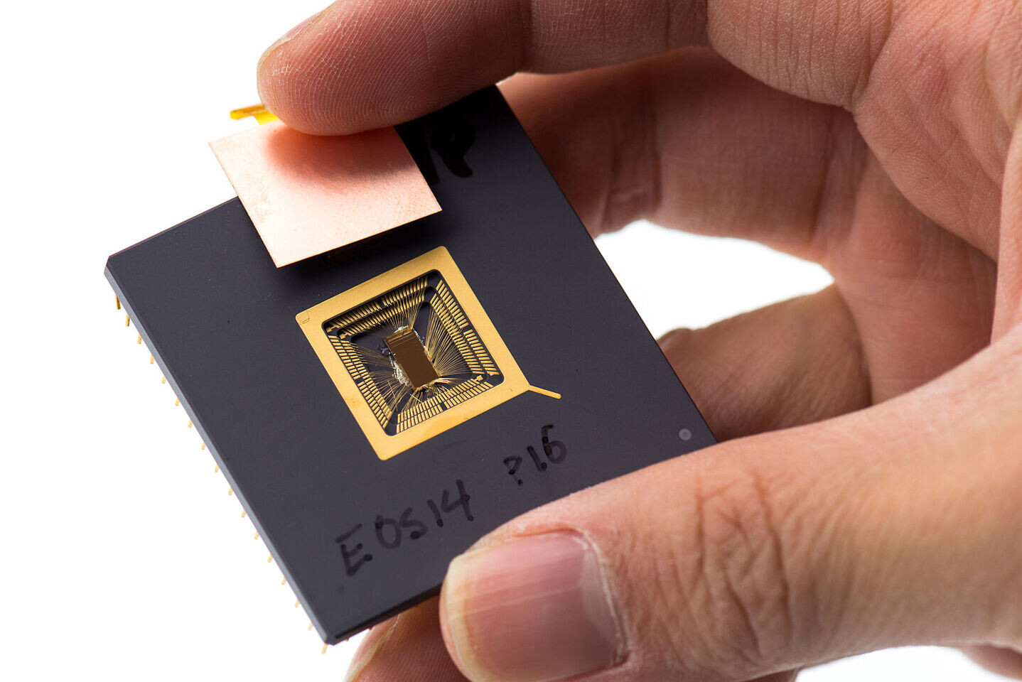
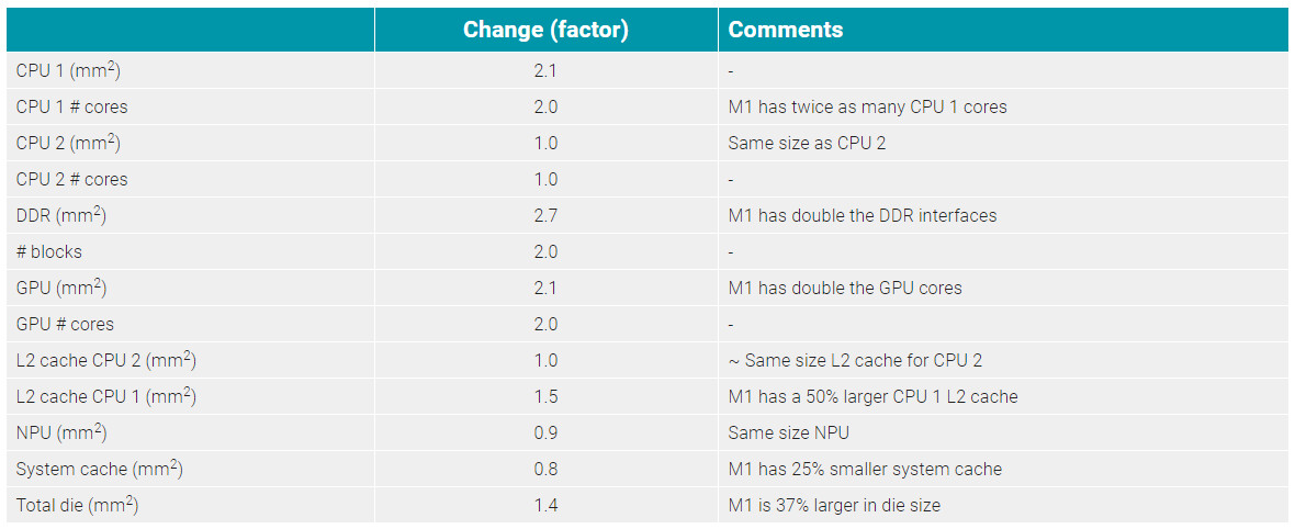
Apple has today patented a new approach to how it uses memory in the System-on-Chip (SoC) subsystem. With the announcement of the M1 processor, Apple has switched away from the traditional Intel-supplied chips and transitioned into a fully custom SoC design called Apple Silicon. The new designs have to integrate every component like the Arm CPU and a custom GPU. Both of these processors need good memory access, and Apple has figured out a solution to the problem of having both the CPU and the GPU accessing the same pool of memory. The so-called UMA (unified memory access) represents a bottleneck because both processors share the bandwidth and the total memory capacity, which would leave one processor starving in some scenarios.

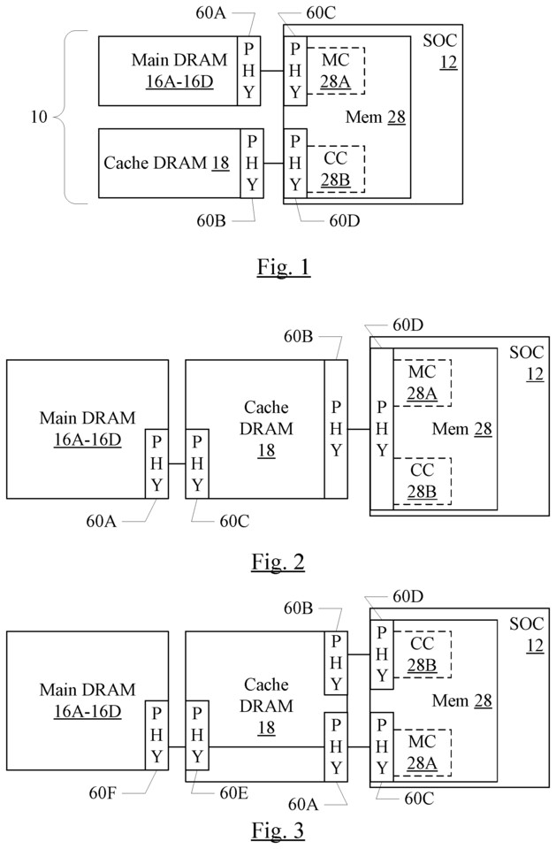
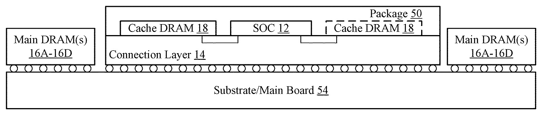
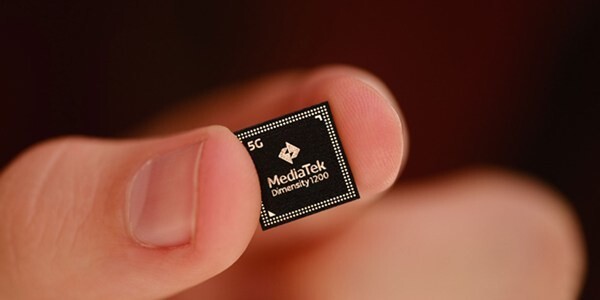
Apple has patented a design that aims to solve this problem by combining high-bandwidth cache DRAM as well as high-capacity main DRAM. "With two types of DRAM forming the memory system, one of which may be optimized for bandwidth and the other of which may be optimized for capacity, the goals of bandwidth increase and capacity increase may both be realized, in some embodiments," says the patent, " to implement energy efficiency improvements, which may provide a highly energy-efficient memory solution that is also high performance and high bandwidth." The patent got filed way back in 2016 and it means that we could start seeing this technology in the future Apple Silicon designs, following the M1 chip.

Update 21:14 UTC: We have been reached out by Mr. Kerry Creeron, an attorney with the firm of Banner & Witcoff, who provided us with additional insights about the patent. Mr. Creeron has provided us with his personal commentary about it, and you can find Mr. Creeron's quote below.

MediaTek Launches 6nm Dimensity 1200 Premium 5G SoC

MediaTek today unveiled its new Dimensity 1200 and Dimensity 1100 5G smartphone chipsets with unrivaled AI, camera and multimedia features for powerful 5G experiences. The addition of the 6 nm Dimensity 1200 and 1100 chipsets to MediaTek's 5G portfolio gives device makers a growing suite of options to design highly capable 5G smartphones with top of the line camera features, graphics, connectivity enhancements and more.

"MediaTek continues to expand its 5G portfolio with highly integrated solutions for a range of devices from the high-end to the mid-tier," said JC Hsu, Corporate Vice President and General Manager of MediaTek's Wireless Communications Business Unit. "Our new Dimensity 1200 stands out with its impressive 200MP camera support and advanced AI capabilities, in addition to its innovative connectivity, display, audio and gaming enhancements."

Apple M1 & A14 Die Shot Comparison Shows Differences in SoC Design

When Apple first announced the M1, questions arose about the differences between it and the A14 chip which both share many architectural features and are both manufactured on TSMC's 5 nm process. Semiconductor analysis firm TechInsights has recently published die photos of the two processors and a summary of the changes.

The M1 features four high-performance Firestorm cores and four energy-efficient IceStorm cores for a total of eight CPU cores. The A14 only features six CPU cores with two high-performance Firestorm cores and four energy-efficient IceStorm cores. The M1 includes doubles the amount of GPU cores and DDR interfaces then found on the A14. The M1 also incorporates silicon not found on the A14 including the Apple T2 security processor and other controllers. These additions result in a die size 37% larger than the A14.

Akasa Rolls Out Turing A50 Case for ASUS PN50 Ryzen 4000-powered Mini PC

Akasa ended the year with the release of the Turing A50, a fanless all-aluminium case with which you can replace the case that comes with the ASUS PN50 mini-PC. The ASUS PN50, if you recall, is a NUC-sized mini-PC that uses 15-Watt AMD Ryzen 4000-series "Renoir" mobile processors. The Akasa Turing A50 is a variation of the original Turing NUC case the company released back in February 2019, but with its innards re-designed for the ASUS PN50 mainboard. On the front side, you get mounts for the board's headset jack, two USB 3.2 ports (from which one is type-C and has DisplayPort passthrough), and the IR receiver. The rear has mounts for the three other display outputs, and a couple more USB ports, and the DC power input. Internally, the case features an SoC cooler base designed to mount onto the "Renoir" SoC, from which a few copper heat-pipes convey heat to the case's aluminium body, which doubles up as a heatsink. Fanless Tech reports that the case should be available from February 2021.

Intel Debuts 2nd-Gen Horse Ridge Cryogenic Quantum Control Chip

At an Intel Labs virtual event today, Intel unveiled Horse Ridge II, its second-generation cryogenic control chip, marking another milestone in the company's progress toward overcoming scalability, one of quantum computing's biggest hurdles. Building on innovations in the first-generation Horse Ridge controller introduced in 2019, Horse Ridge II supports enhanced capabilities and higher levels of integration for elegant control of the quantum system. New features include the ability to manipulate and read qubit states and control the potential of several gates required to entangle multiple qubits.

"With Horse Ridge II, Intel continues to lead innovation in the field of quantum cryogenic controls, drawing from our deep interdisciplinary expertise bench across the Integrated Circuit design, Labs and Technology Development teams. We believe that increasing the number of qubits without addressing the resulting wiring complexities is akin to owning a sports car, but constantly being stuck in traffic. Horse Ridge II further streamlines quantum circuit controls, and we expect this progress to deliver increased fidelity and decreased power output, bringing us one step closer toward the development of a 'traffic-free' integrated quantum circuit."-Jim Clarke, Intel director of Quantum Hardware, Components Research Group, Intel.

Intel Sells Its Power Management Chip Business, Enpirion, to Mediatek for $85 Million

Intel continues to "shed fat" on its business portfolio. After last year's sale of its smartphone modem chip business to Apple, the company is now parting ways with its power management circuitry division - Enpirion - and offloading it to Richtek, a division of Taiwanese MediaTek. The sale price of $85 million is a drop in the bucket for Intel's overall bottom line, so it's not a way for the company to cash in some desperately needed money - all accounts of Intel's troubles in the wake of its semiconductor manufacturing issues and AMD's market resurgence pale in comparison to Intel's revenues.

This actually looks like a company that's actually streamlining its R&D expenditures and focusing on execution for the markets Intel sees as most important for today and for tomorrow. Intel's Enpirion focuses on building power management chips for FPGA circuits, SoCs, CPUs, and ASICs, and will now serve to bolster MediaTek's SoC business while allowing the Taiwanese company to expand and diversify its business portfolio, even as Intel focuses on their core competencies.

Samsung Could Become Apple's Newest Chip Supplier

Apple has recently announced its transition to Apple Silicon, meaning that every processor inside its products will be custom designed by the company. However, that seems to be becoming a bit of a problem. The sole supplier of chips for Apple has been Taiwan Semiconductor Manufacturing Company (TSMC), which Apple collaborated with for the past few years. The sheer capacity of TSMC is enough to satisfy the demand from several companies and thus it allows some of them to book its capacity. With Apple demanding more and more capacity than ever before, it is becoming quite hard to keep up with it. That is why Apple is, according to some analysts for Business Korea, looking for a foundry beyond TSMC's to manufacture its chips.

According to the source, Apple is looking at the direction of Samsung Electronics and its silicon manufacturing facilities. Samsung has recently started the production of its 5 nm silicon manufacturing node. We have reported that the first SoCs are set to arrive soon. However, it may be possible that Apple's M1 lineup of SoCs will be a part of that first wave. Apple is reportedly going to tap both TSMC and Samsung to qualify enough supply for the huge demand of the products based on the latest 5 nm technology.

MediaTek Announces Dimensity 700 SoC For Mass Market 5G Smartphones

MediaTek today unveiled its new Dimensity 700 5G smartphone chipset, a 7 nm SoC designed to bring advanced 5G capabilities and experiences to the mass market. The addition of the Dimensity 700 to MediaTek's Dimensity family of 5G chips gives device makers a full suite of options for 5G smartphone models - from flagship and premium to mid-range and mass market devices - making 5G more accessible for consumers everywhere.

"With our expanded Dimensity portfolio we're bringing the latest 5G capabilities to every smartphone tier so more people can enjoy 5G experiences," said Dr. JC Hsu, Corporate VP and GM of MediaTek's Wireless Communications Business Unit. "The Dimensity 700 has an impressive mix of 5G connectivity features, advanced camera capabilities like night shot enhancements and multiple voice assistant support, all in a super power-efficient design."

Apple Could Unveil Arm-powered MacBooks on November 10

Apple late Monday sent out a public invite to an online launch event dated November 10, without revealing what it is. With new generation iPhones and Watches and iPads already announced it's likely that the November 10 event could deal with Macs, specifically, the company's very first MacBooks powered by a non-Intel processor since the company embraced x86 some decade-and-a-half ago.

Apple, having gained in-house expertise in designing powerful Arm-based SoCs, is likely to debut a new Arm-based processor with sufficient muscle to drive MacBooks, in what will be a "client-first" strategy of replacing x86 with Arm for Apple. This will likely see the most client-segment products, such as MacBooks and Mac Mini, get the processor, followed by MacBook Pros, iMacs, and lastly workstation-segment products such as the Mac Pro and iMac Pro. The November 10 event will likely only cover the very first Arm-powered MacBooks. Apple has been selling Arm-powered Mac Minis to ISVs along with a special version of macOS "Big Sur," so they could port their Mac software to the new platform. Arm-powered Macs could also see some form of unification between the iOS and macOS software ecosystems.
Return to Keyword Browsing
Feb 19th, 2025 17:13 EST change timezone

New Forum Posts

Popular Reviews

Controversial News Posts