Monday, February 15th 2021

Sony Playstation 5 SoC Die Has Been Pictured
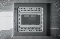
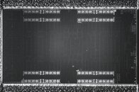
When AMD and Sony collaborated on making the next generation console chip, AMD has internally codenamed it Flute, while Sony codenamed it Oberon or Ariel. This PlayStation 5 SoC die has today been pictured thanks to the Fritzchens Fritz and we get to see a closer look at the die internals. Featuring eight of AMD's Zen2 cores that can reach frequencies of up to 3.5 GHz, the CPU is paired with 36 CU GPU based on the RDNA 2 technology. The GPU is capable of running at speed of up to 2.23 GHz. The SoC has been made to accommodate all of that hardware, and bring IO to connect it all.
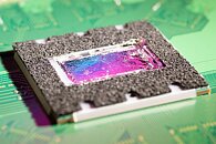
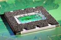
When tearing down the console, the heatsink and the SoC are connected by liquid metal, which is used to achieve the best possible heat transfer between two surfaces. Surrounding the die there is a small amount of material used to prevent liquid metal (a conductive material) from possibly spilling and shorting some components. Using a special short wave infrared light (SWIR) microscope, we can take a look at what is happening under the hood without destroying the chip. And really, there are a few distinct areas that are highlighted by the Twitter user @Locuza. As you can see, the die has special sectors with the CPU complex and a GPU matrix with plenty of workgroups and additional components for raytracing.According to the photographer, there are also a few components missing compared to the original Zen 2 design, with that being the Fixed Function Units (FFU) and Fused Multiply-Add (FMA/FMADD) functions likely not needed for the gaming console. According to the Twitter user Locuza, Sony has cut down the floating-point pipeline from 256-bit width to 128-bit wide bus. Another important note is that there is no L3 cache (Infinity Cache) being present, just like it is missing on Xbox Series X SoC as well. You can take a look at the die for yourself below.
Sources:
Fritzchens Fritz, Locuza, via VideoCardz
When tearing down the console, the heatsink and the SoC are connected by liquid metal, which is used to achieve the best possible heat transfer between two surfaces. Surrounding the die there is a small amount of material used to prevent liquid metal (a conductive material) from possibly spilling and shorting some components. Using a special short wave infrared light (SWIR) microscope, we can take a look at what is happening under the hood without destroying the chip. And really, there are a few distinct areas that are highlighted by the Twitter user @Locuza. As you can see, the die has special sectors with the CPU complex and a GPU matrix with plenty of workgroups and additional components for raytracing.According to the photographer, there are also a few components missing compared to the original Zen 2 design, with that being the Fixed Function Units (FFU) and Fused Multiply-Add (FMA/FMADD) functions likely not needed for the gaming console. According to the Twitter user Locuza, Sony has cut down the floating-point pipeline from 256-bit width to 128-bit wide bus. Another important note is that there is no L3 cache (Infinity Cache) being present, just like it is missing on Xbox Series X SoC as well. You can take a look at the die for yourself below.


13 Comments on Sony Playstation 5 SoC Die Has Been Pictured
The only ways it can dry out is with a chemical reaction at this point. Even if it freezes, it will return to liquid once the tempature rises again.Thermal Grizzly Conductonaut at least doesn't do well on copper, but nickel plated copper has always been fine with me. Copper is fine too if you don't mind reapplying a few times after the first few failed coats form a layer to protect it.
It stains everything of course, but that's a given.
I'll no doubt get a PS5 (when scalpers get bored of buying up the stock), past history has taught me that Sony do tend to update the systems a fair bit though.