News Posts matching #TSMC

Return to Keyword Browsing

TSMC Reports Fourth Quarter EPS of NT$1.22

TSMC today announced consolidated revenue of NT$104.71 billion, net income of NT$31.58 billion, and diluted earnings per share of NT$1.22 (US$0.20 per ADR unit) for the fourth quarter ended December 31, 2011.

Year-over-year, fourth quarter revenue decreased 4.9% while both net income and diluted EPS decreased 22.5%. Compared to third quarter of 2011, fourth quarter of 2011 results represent a 1.7% decrease in revenue, and a 3.9% increase in both net income and diluted EPS. All figures were prepared in accordance with R.O.C. GAAP on a consolidated basis.

In US dollars, fourth quarter revenue decreased 5.4% from the previous quarter and decreased 4.5% year-over-year. Gross margin for the quarter was 44.7%, operating margin was 31.4%, and net margin was 30.2%.

AMD Denies Hidden GCN CUs in Tahiti

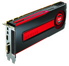
Over the past few days, we were hearing rumors from many quarters that AMD's "Tahiti" high-performance GPU may have been a deviation from an older specification, and that it really has 2304 stream processors spread across 40 GCN compute units (CUs), instead of the 32 the Radeon HD 7970 ended up with. Both AMD and NVIDIA create more redundant components on their chips than their SKUs end up getting, so they could increase yields, it's a process commonly known as "harvesting".

On Tuesday, AMD quashed the rumor in an e-mail to Bright Side of News, in which it said that Tahiti XT (Radeon HD 7970) makes use of all the CUs there are, on the chip. The 40 CU / 2308 SP rumor gained some weight with the fact that since AMD is venturing into unknown territory (TSMC's 28 nm process, built after quite some delays and failures), it could do some heavy harvesting. Examples of harvesting in recent past include Intel Sandy Bridge-E Core i7 processors, which use only up to 6 out of 8 cores on the silicon, and only up to 15 MB out of 20 MB available on it; and GeForce GTX 480, which used only 480 out of 512 CUDA cores available on the GF100 GPU.

Taiwan Foundries Cut Prices

Taiwan foundries are going to be cutting prices by 10 to 15% for wafers built on mature node processes. Since these wafers have lower production costs the foundries are passing on the savings. This move is to boost consumer confidence in building their inventory after a year of shaky ground in the U.S. and European markets. This according to DigiTimes.

Also DigiTimes is reporting despite slow demand for mature process manufacturing, Taiwan Semiconductor Manufacturing Company (TSMC) continues to see orders heat up for advanced 28nm technology, according to sources at non Taiwan-based chip suppliers.

This news could mean that these same vendors that are getting a cut in overhead thanks to the foundries could pass on the savings to the end customer to boost revenue.

TSMC 18-inch Wafer Volume Production On Course for 2015

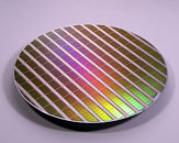
TSMC told industry observers that its plans to test large 18 inch wafers are on schedule for 2012-13, and should reach volume production in 2015. Silicon chips are manufactured on large discs known as wafers, and cut out of them. Like pizza, the sizes of wafers are measured by their diameters. The 18 inch diameter wafer has been something TSMC has been working on. Larger the wafer, the more chips can be cut out of a single wafer. It works to reduce production costs. TSMC expects to have 95% of its 18 inch wafer production equipment installed in 2014, and commence volume production by 2015. Currently, TSMC faces technical hurdles that have to be solved in collaboration with equipment and material suppliers.

AMD Radeon HD 7900 Key Features Listed

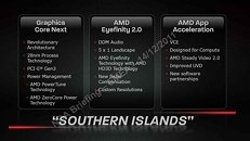
We've already been through the specifications of HD 7970 "Tahiti" in some detail that matters to those who can draw a performance hunch looking at them. This latest slide shows you the feature-set this GPU comes with. To begin with, there are three main categories of feature updates: Graphics CoreNext, AMD Eyefinity 2.0, and AMD APP Acceleration. AMD claims CoreNext to be a "revolutionary" new architecture that changes the way the GPU crunches numbers.

For the past five generations (since Radeon HD 2000), AMD GPUs have used the VLIW (very-long instruction word) core arrangement. Even the latest VLIW4 introduced by Radeon HD 6900 series, was an evolution, than a revolution of that. CoreNext replaces VLIW stream processors with super-scalar Graphics Compute cores. This should translate to higher performance per mm² die-area, resulting in smaller GPUs, giving AMD room for greater cost-cutting if the competition from NVIDIA for this generation takes effect. The GPU itself is built on TSMC's new 28 nm silicon fabrication process. Next up, AMD confirmed support for PCI-Express 3.0 interface, that nearly doubles system bus bandwidth over the previous generation.

AMD Starts Shipping 28 nm GPUs for Revenue

AMD CEO Rory Read, speaking at the IT Supply Chain conference organized by Raymond James this Tuesday, said that his company had begun shipping 28 nm GPUs for revenue (meaning, in volumes big enough to fetch revenue). With it, AMD fulfilled its promise to be the first to the market with GPUs built on the 28 nm silicon fab process. AMD's foundry partner for these chips is TSMC. "We are ramping 28nm [products] with TSMC in Taiwan and shipping the products here and now. We are very excited about the products," said Read.

At the upcoming CES event, AMD will formally unveil a range of products that will use its 28 nm GPUs. CES will give AMD a good opportunity to bag design wins with large volume manufacturers of notebooks and PCs. What this means for the enthusiast community is that whenever AMD does launch its Radeon HD 7900 series, it won't be a "paper-launch".

GeForce Kepler 104 and 100 GPU Specifications Compiled

A quick stroll through our previous article about how the GeForce Kepler family of next-generation GPUs is laid out, would tell you that GeForce Kepler 104 (GK104), is going to be NVIDIA's answer to AMD's Tahiti. GK104 will be a high-performance (≠ high-end) GPU by NVIDIA that will have many of the features that were reserved for its previous high-end GPUs (such as a 384-bit wide GDDR5 memory interface), but will not be NVIDIA's most powerful GPU in the series. The throne will be kept empty for GK100, which will comply with NVIDIA's "go all in" design ideology for high-end GPUs.

3DCenter.org compiled a few specifications of the GK104 and GK100. They go like this:
GK104
  • 640 to 768 CUDA cores
  • 80 to 96 TMUs (depending on what the CUDA core count ends up being)
  • 384-bit GDDR5 memory interface, 48 ROPs
  • Built on the 28 nm TSMC process
  • Products based on this will launch in the first quarter of 2012

AMD Tahiti GPU Specifications Compiled

If the word on the optical fibers is true, we are less than a month away from the launch of AMD's next high-end graphics card family based on its next high-performance GPU, codenamed "Tahiti". According to 3DCenter, AMD will launch new graphics card models based on this GPU around January 10, 2012. It is expected that we'll learn a lot more about these GPUs, maybe even come across AIB-branded graphics cards, at the upcoming CES event.

3DCenter compiled specifications of "Tahiti", based on bits and pieces of information from various sources. The specs can be listed out as:
  • 4.50 billion transistors, die-area of 380 mm², built on TSMC 28 nm process
  • Advanced GCN 1D architecture
  • 2048 1D processing cores
  • 128 TMUs, 48 ROPs
  • 384-bit wide GDDR5 memory interface, memory clock slightly below 1 GHz, target bandwidth of 240~264 GB/s
In Gandhi's words, salt is as free as the air.

NVIDIA GeForce Kepler Roadmap Compiled

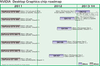
2012-13 promises to be a period of big graphics product launches, centric to a new DirectX version, DirectX 11.1, which will ship with Microsoft's next major Windows version (currently referred to as Windows 8). Information compiled by ExpertsPC.com and 4Gamer.net tables what NVIDIA's next-generation graphics family could look like, and around what time it could be released to market. With its next-generation GeForce Kepler family of GPUs, NVIDIA will follow a sensible bottom-up product release model, to ensure that it isn't met with any technical hurdles with TSMC's new 28 nm manufacturing process, and so it could launch GPUs with increasingly higher transistor counts, till its top-of-the-line GPU is outed.

The first GPU in NVIDIA's pipeline is the GeForce Kepler 107 (GK107), on which will be based entry thru lower-mainstream SKUs. The data doesn't reveal things like core counts, but points out that GK107 will have a 128-bit wide GDDR5 memory interface, will use the current-generation PCI-Express 2.0 bus, will be built on the 28 nm process, and will support DirectX 11.1. This will be followed by the GK106, on which "sweet-spot" SKUs could be based. This will be NVIDIA's first PCI-Express 3.0 compliant GPU, it will have a 256-bit wide GDDR5 memory interface.

Are Improving Integrated Graphics Slowly Killing Off Discrete Graphics Cards?

Intel started the trend of improving integrated graphics with their second generation LGA1155 socket Core i3, i5 & i7 line of processors. Depending on the model, these processors sport integrated HD2000 or HD3000 graphics right on the processor die, which nowadays give acceptable performance for low-end gaming and can play Full HD 1080p video perfectly. This trend is increasing with the upcoming Ivy Bridge processors, which will be able to support a massive 4096 x 4096 pixel display, as we reported here. AMD now also have equivalent products with their Llano-based A-series processors. So, where does this leave discrete graphics cards? Well, the low end market is certainly seeing reduced sales, as there really isn't enough of a performance difference nowadays to always warrant an upgrade from an IGP. As integrated graphics improve further, one can see how this will hurt sales of higher end graphics cards too. The problem is that the bulk of the profit comes not from the top-end powerhouse graphics cards, but from the low to mid-end cards which allow these companies to remain in business, so cannibalizing sales of these products to integrated graphics could make high-end graphics cards a much more niche product and crucially, much more expensive with to boot.

TSMC 28 nm Technology in Volume Production

TSMC today announced that its 28nm process is in volume production and production wafers have been shipped to customers. TSMC leads the foundry segment to achieve volume production at 28nm node.

TSMC's 28nm process offering includes 28nm High Performance (28HP), 28nm High Performance Low Power (28HPL), 28nm Low Power (28LP), and 28nm High Performance Mobile Computing (28HPM). Among these technology offerings, 28HP, 28HPL and 28LP are all in volume production and 28HPM will be ready for production by the end of this year. The production-version design collateral of 28HPM has been distributed to most mobile computing customers for their product-design use.

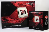
AMD to Turn to TSMC for ''Bulldozer'' Manufacturing

AMD is rumored to be seeking ties with TSMC, Taiwan's premier semiconductor manufacturing foundry, for future manufacturing of its "Bulldozer" architecture processors, according to a report by DonanimHaber. This has two very distinct implications: first, AMD could be facing issues with GlobalFoundries 32 nm HKMG node, its de facto foundry for CPU manufacturing, and second, this could just be an obvious development of future low-power APUs based on the new x86 architecture being manufactured at TSMC, much like how current E-series and C-series APUs are.

Then again, AMD doesn't exactly have any APUs in works that use "Bulldozer" architecture for the x86 cores, rather, its successor codenamed "Piledriver". Another couple of important things to note here are that TSMC does not have a 32 nm bulk node (it was scrapped with the transition to 28 nm bulk), and its HKMG (high-K metal gate transistor) manufacturing technology is deployed rather recently. It would be interesting to follow this development.

GeForce BETA Driver Hints At First GeForce 600 Series Models

If not mission-critical stability, GeForce BETA drivers do tend to be great speculation starters. The driver information file packs entries for existing supported GPUs, as well as some future GPUs. GeForce 285 BETA drivers seem to have contained entries for two such future GPUs, marked "NVIDIA GeForce 610M" and "NVIDIA GeForce GT 630M", with identifications of NVIDIA_DEV.1058.01 and NVIDIA_DEV.0DE9.01, respectively.

These new "discoveries" more or less fall in line with an earlier report of NVIDIA having taped out its first GeForce Kepler family GPU, the GK107. It is becoming clear that NVIDIA has charted out a bottom-up course for its next GPU family, to play safe with the new 28 nm fabrication processes at TSMC, that of beginning with the simplest GPUs, and then scaling them up till the highest-performing part is perfected.

NVIDIA Begins Sampling First Kepler GPUs

Graphics major NVIDIA has begun sampling the first GPUs of its next-generation Kepler family. Kepler succeeds the present generation Fermi family of GPUs, that make up the GeForce 400 and 500 series. Members of the GeForce Kepler family will follow the codename nomenclature of GK1xx, like GeForce Fermi followed GF1xx. The first GPU being sampled is codenamed GK107. The codename suggests that this isn't the top-end part, it's more like a lower-mainstream or value segment offering.

It is reported that GK107 has a 128-bit GDDR5 memory bus, which also supports inexpensive DDR3 memory. It is built in small quantities on TSMC's 28 nanometer fab process (as the foundry isn't ready for 28 nm bulk manufacturing. NVIDIA will follow a "bottom-to-top" strategy, when dealing with a new fab process technology. It will first design the smallest, simplest GPUs in the lineup, and then gradually move on to larger ones. The first GK107-based SKUs will succeed the GeForce GT 500M series. NVIDIA will carve out four SKUs, internally, NVIDIA will refer to those as N13P-LP, N13P-GS, N13P-GT and N13E-GE, with N13E-GE being the "enthusiast" part. Its market SKU will likely succeed the GeForce GT 560M.

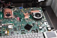
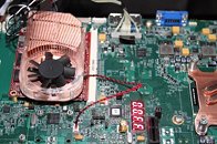
AMD Showcases its First 28 nm GPU

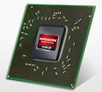
AMD showed off its first graphics processor (GPU) built on TSMC's cutting-edge 28 nanometer silicon fabrication process, the next foundry process standard for discrete GPUs. Bulk manufacturing at TSMC's Fab 15 facility at 28 nm is still taking shape, TSMC will take volume orders only later this year. For the moment, it can run small batches for designers to test their designs. The GPU was running on a mobile platform (pictured below, the red PCB), cooled by a compact copper-channel air cooler, leading us to believe that this is a mainstream segment GPU, if not lower. The demo platform was showcased running DirectX 11 title Dirt 3. Besides that, absolutely no other details were shared, not even a company codename for the GPU board.

AMD Radeon HD 7000 Series to be PCI-Express 3.0 Compliant

AMD's next generation of graphics processors (GPUs) that will be branded under the HD 7000 series, are reported to be PCI-Express Generation 3 compliant. The desktop discrete graphics cards will feature PCI-Express 3.0 x16 bus interfaces, and will be fully backwards-compatible with older versions of the bus, including Gen 1 and Gen 2. Motherboards sold today feature Gen 2 PCI-E slots, although some of the very latest motherboards launched by major vendors feature PCI-Express 3.0 slots.

The new bus doubles the bandwidth over PCI-E 2.0, with 1 GB/s of bandwidth per lane, per direction. PCI-Express 3.0 x16 would have 32 GB/s (256 Gbps) of bandwidth at its disposal, 16 GB/s per direction. AMD's next generation of GPUs, codenamed "Southern Islands" will be built on the new 28 nm process at TSMC, and will upscale VLIW4 stream processors. Some of the first PC platforms to fully support PCI-Express 3.0 will be Intel's Sandy Bridge-E. Whether AMD's GPUs have hit a bandwidth bottleneck with PCI-E Gen 2, or is AMD trying to just be standards-compliant, is a different question altogether.

Foundry Delays to Push Back NVIDIA Kepler Launch to 2012

It looks like foundry issues are back to slow down the launch of NVIDIA's next generation high-end GPU, codenamed Kepler. The delay may push Kepler's launch to 2012, it was expected to launch by late 2011. The 28 nanometer silicon fabrication process at TSMC, a principal foundry partner of NVIDIA, is producing unsatisfactory yields. Add to that, Kepler's performance is lower than expected.

TSMC's 28 nm process at Fab 15 facility has already seen delays, which have even shaped AMD's designs in a big way. AMD had originally planned to design high-end VLIW4 chips on the 32 nm process at TSMC, but later decided to wait for the 28 nm process, leading to plans of 32 nm GPUs being scrapped by both GPU designers. TSMC was supposed to be in a position take orders of high-end 28 nm GPUs by Q4 2011, and was set to start pilot production for its 20nm process technology in the third quarter of 2012.

Acer Readying Tablets Based on AMD Z-Series APUs

Acer has just placed an order for 80,000 pieces of AMD Z-series accelerated processing units. Based on essentially the same design as Fusion "Zacate", Z-series APUs are designed to have lower TDP and to be of higher quality, so they could be deployed in enterprise and IPC (industrial PC) environments. The AMD Z-01 is Acer's choice, this chip combines two x86-64 cores clocked at 1.00 GHz with AMD Radeon HD 6250 DirectX 11 compliant graphics, and a DDR3 memory controller. The TDP of the entire chip stands at 5.9W, it is built on the 40 nm process at TSMC.

Acer's first tablets based on AMD Z-01 will run Windows 7, since Android 3.0 (codenamed "Ice Cream Sandwich") is not going to be out any time before the end of 2011. Acer isn't the only big tablet-maker opting for AMD Z-series over Intel's Atom Pine Trail platform, MSI is also reported to be working on x86 tablets running AMD Z-series. Manufacturers are opting for Z-series over Pine Trail, because the latter has both higher price and TDP. With its relatively faster iGPU, Z-series should be able to drive graphics-intensive custom user-interfaces on tables sized up to 10.1-inches. Industry sources expect AMD to ship up to 500,000 units of the chip in the second half of 2011.

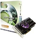
SPARKLE Debuts GeForce GTX 560 Graphics Cards

SPARKLE Computer Co., Ltd., the professional VGA card manufacturer and supplier, today debut the SPARKLE GeForce GTX 560 Graphics Cards, which are designed for mainstream users looking to build the premium PC gaming rig. Thanks to the improved 40nm core manufacturing process at TSMC, now the SPARKLE GeForce GTX 560 Graphics Cards have outstanding performance power consumption ratio than ever. Compared with previous generation products, the SPARKLE GeForce GTX 560 Graphics Cards also feature a special cooling system and a hardware power monitor circuit which deliver higher performance/Watt ratio. Tested in SPARKLE R&D lab, the SPARKLE GeForce GTX 560 Graphics Cards have the same power consumption as GeForce GTX 460 graphics card, but providing 28% more performance in today hottest games.

Sparkle Announces its GeForce GTX 550 Ti Graphics Card

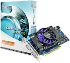
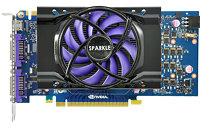
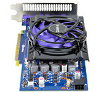
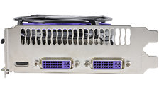
SPARKLE Computer Co., Ltd., the professional VGA card manufacturer and supplier, today presents The SPARKLE GeForce GTX 550 Ti Graphics Card, -- the latest product of SPARKLE GTX 500 Series. It delivers performance upgrade for mainstream DX11 gamers. Using the advanced Fermi 2.0 architecture from NVIDIA, the SPARKLE GeForce GTX 550 Ti Graphics Card upgrades core algorithms such as texture filtering and Z-axis compression over Fermi 1.0 architecture, so that the corresponding instruction operation efficiency is greatly enhanced. With 40nm manufacturing process improvements, now the SPARKLE GeForce GTX 550 Ti Graphics Card features higher core clock than GeForce GTS 450 graphics cards. With the two improvements, the Performance/Watt ratio of the SPARKLE GeForce GTX 550 Ti Graphics Card is 20% better over the GeForce GTS 450 graphics cards.

TSMC Reiterates 28 nm Readiness by Q4 2011

TSMC reiterated that it will be ready with a 28 nanometer manufacturing process by Q4 2011. The semiconductor company handles manufacturing of graphics processors for both AMD and NVIDIA. After the current 40 nm process, 32 nm, the next milestone process, was canceled for GPU makers to leap to 28 nm, this caused the foundry transition to the next process to take longer than usual. The current 40 nm process already seems to be saturated by GPUs with over 3 billion transistors, which are barely able to maintain acceptable thermal specs without using some sort of power-load throttling mechanism.

TSMC Chairman and CEO, Morris Chang, confirmed that tape-outs will be starting as early as in Q3, and production of 28 nm chips will start in Q4. Chang expects that up to 3% of TSMC's revenues will be made from 28 nm chips by the end of the year. "We plan to have around 2% or 3% of our total revenue in the fourth quarter [to] be 28nm. The tape-outs of the 28-nanaometer will start to ramp in the second half, starting in the third quarter and then more in the fourth quarter. But the real momentum [for 28nm], we believe, will be next year," Chang said. Apart from GPUs, the 28 nm process will also benefit ARM processors, with multi-core ARM chips clocked at 3 GHz being on cards. The 28 nm bulk process will also dish out AMD's next generation accelerated processing units (APUs).

Sparkle Announces Calibre X560 Graphics Card

SPARKLE Computer Co., Ltd., the professional VGA card manufacturer and supplier, announced the Calibre X560 Graphics Card with Accelero cooling solution from Arctic Cooling, delivering unparalleled levels of cooling performance and gaming experience to mainstream gamers. The Calibre X560 Graphics Card adopts the Fermi 2.0 architecture which upgrades core algorithms such as texture filtering and Z-axis compression over Fermi 1.0 architecture, so that the corresponding instruction operation efficiency is greatly enhanced. At the same time, with semiconductor chip manufacturing technology improvements at TSMC, through the upgrading of core components and semiconductor manufacturing process optimization of its characteristics, still based on TSMC 40nm process in the premise, The Calibre X560 Graphics Card can run at higher frequencies. By the two improvements, the Performance/Watt ratio of the Calibre X560 Graphics Card has great increase over GeForce GTX 470 graphics cards.

NVIDIA and TSMC Ship One-Billionth GeForce Graphics Processor

NVIDIA and TSMC today celebrated the shipment of the one-billionth GeForce graphics processor designed by NVIDIA and manufactured by TSMC. Today's announcement is a testament to the popularity of GeForce graphics processors, which are recognized worldwide for exceptional performance in games, video, and nearly all forms of 3D content. Today nearly every major PC manufacturer offers systems powered by GeForce GPUs.

The partners achieved the one-billionth processor milestone in less than 12 years. This achievement reflects a shared commitment to technological excellence and a relentless pace of innovation. Through deep trust and long-term objectives, the companies have raised the bar for the ambitions and practices that have helped shape the semiconductor industry.

ATI Radeon HD 6000 Series ''Southern Islands'' Graphics Cards For Sale from November

Come this Winter, and things will heat up once again in the graphics card industry, with GPU vendors battling it out for the crucial Holidays shopping season. While AMD did not introduce any new GPUs after completing its ATI Radeon HD 5000 series launch itinerary, it did manage to grab significant amount of sales from its graphics rival NVIDIA. For this Winter, AMD and its partners will be in a position to launch the ATI Radeon HD 6000 series graphics processors, according to DigiTimes, citing sources from graphics card vendors.

It is also said that the Radeon HD 6000 series, codenamed "Southern Islands" (members of which are codenamed after islands in the Mediterranean Sea), will be built on TSMC's 40 nm manufacturing process. AMD had originally planned to build Southern Islands on TSMC's 32 nm process, but with the foundry skipping 32 nm bulk for 28 nm which will start operations only by the end of the year, AMD redrew its plans and stuck to the now-mature (stable) 40 nm process. Perhaps AMD learned a thing or two from a wide range of teething problems that plagued the 40 nm production line.

TSMC Reports Second Quarter EPS of NT$1.55

TSMC announced consolidated revenue of NT$104.96 billion, net income of NT$40.28 billion, and diluted earnings per share of NT$1.55 (US$0.24 per ADS unit) for the second quarter ended June 30, 2010. Year-over-year, second quarter revenue increased 41.4% while net income increased 64.8% and diluted EPS increased 65%. Compared to first quarter of 2010, second quarter results represent a 13.9% increase in revenue, and a 19.7% increase in both net income and diluted EPS. All figures were prepared in accordance with R.O.C. GAAP on a consolidated basis.

Gross margin for the quarter was 49.5%, operating margin was 38.6%, and net margin was 38.4%. In the second quarter, demand for TSMC's wafers continued to be strong, and wafer shipments in all major semiconductor market segments increased from their first quarter levels. Advanced process technologies (0.13-micron and below) accounted for 72% of wafer revenues. 90-nanometer process technology accounted for 16% of wafer revenues, 65-nanometer 27%, and 40-nanometer 16% of total wafer sales.
Return to Keyword Browsing
Apr 22nd, 2025 10:21 EDT change timezone

New Forum Posts

Popular Reviews

Controversial News Posts