News Posts matching #TSMC

Return to Keyword Browsing

TSMC and ARM Tape-Out First ARM Cortex-A57 Processor on 16 nm FinFET Technology

TSMC and ARM today announced the first tape-out of an ARM Cortex-A57 processor on FinFET process technology. The Cortex-A57 processor is ARM's highest performing processor, designed to further extend the capabilities of future mobile and enterprise computing, including compute intensive applications such as high-end computer, tablet and server products. This is the first milestone in the collaboration between ARM and TSMC to jointly optimize the 64-bit ARMv8 processor series on TSMC FinFET process technologies. The two companies cooperated in the implementation from RTL to tape-out in six months using ARM Artisan physical IP, TSMC memory macros, and EDA technologies enabled by TSMC's Open Innovation Platform (OIP) design ecosystem.

ARM and TSMC's collaboration produces optimized, power-efficient Cortex-A57 processors and libraries to support early customer implementations on 16 nm FinFET for high-performance, ARM technology-based SoCs.

AMD "Jaguar" Micro-architecture Takes the Fight to Atom with AVX, SSE4, Quad-Core

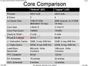
AMD hedged its low-power CPU bets on the "Bobcat" micro-architecture for the past two years now. Intel's Atom line of low-power chips caught up in power-efficiency, CPU performance, to an extant iGPU performance, and recent models even feature out-of-order execution. AMD unveiled its next-generation "Jaguar" low-power CPU micro-architecture for APUs in the 5W - 25W TDP range, targeting everything from tablets to entry-level notebooks, and nettops.

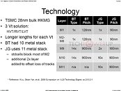
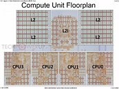
At its presentation at the 60th ISSC 2013 conference, AMD detailed "Jaguar," revealing a few killer features that could restore the company's competitiveness in the low-power CPU segment. To begin with, APUs with CPU cores based on this micro-architecture will be built on TSMC's 28-nanometer HKMG process. Jaguar allows for up to four x86-64 cores. The four cores, unlike Bulldozer modules, are completely independent, and only share a 2 MB L2 cache.

It's Sony, Not AMD in GeForce Titan's Crosshair

When we first heard of NVIDIA launching its GK110-based consumer graphics card by as early as February, it took us by surprise. Intimidating naming (GeForce Titan 780?) aside, the graphics card is hoping to better NVIDIA's current-generation flagship, the dual-GPU GeForce GTX 690, in a single-GPU package, but does the graphics card market really need NVIDIA to launch its card at the moment? Perhaps not, but the answer lies not with AMD and competition in the graphics card market, but Sony, and competition between PC and console platforms.

Over the weekend, it surfaced that Sony would introduce its next-generation PlayStation console (codenamed "Orbis") later this month, and it would mark the beginning of the next-generation of game consoles. PlayStation 4 features an updated hardware feature-set, and promises to raise the bar with graphics detail that the console industry held with an iron fist for the past half decade. This presents a challenge for not only NVIDIA, but PC gaming in general. Here's how.

Intel Shows Off Industry's First Fully-Patterned 450 mm Wafer

At the SEMI Industry Strategy Symposium (ISS) held late last week, Intel unveiled the pride of its fabs, the industry's first fully-patterned (ready to slice) 450 mm wafer. Major semiconductor fabs around the world are locked in a race for who gets volume-production on 450 mm wafers going first. Among the contenders are Taiwan's TSMC, UAE's GlobalFoundries, and Korea's Samsung, and with the unveiling of the first fully-patterned wafer, Intel appears to have announced its lead. The 450 mm (diameter), thanks to its large surface area, significantly increases yields.

"[This] is an important step forward and it indicates that there will soon be substantial volume of patterned test wafers for use by suppliers in developing their 450 mm tools," stated Chuck Mulloy, a spokesperson for Intel. As for what Intel etched on the wafer, a report claims it could be large dies of simple (highly-patterned) devices such as flash. The fab reportedly used Impints' J-Fil imprint lithography technology that demonstrated 24 nm patterning with line edge roughness of less than 2 nm to 3Σ and critical dimension uniformity to 1.2 nm 3Σ, offering the prospect of 10 nm patterning with single-step process.

TSMC Begins Fab 14 Phase 6 Construction

TSMC broke ground for construction of Fab 14 Phase 6, located in Southern Taiwan Science Park (STSP). The new facility will boost the foundry's 12-inch wafer production capacity, leading the way to construction of Phase 7 in 2013. TSMC's facilities in STSP generate 42% of the company's revenues, with a production value of US $6 billion, hiring over 9,000 employees. Phases 1~4 of Fab 14, which specializes in 12-inch wafers, has a quarterly foundry capacity of 540,000 12-inch wafers to produce over 1,200 different types of ICs for about 150 clients a year, according to company executive vice president and co-COO Chiang Shang-yi. In 2013-14, TSMC Fab 14 will become the world's first fab with 20 nanometer SoC volume production, and the company's first plant to start 16 nanometer FinFET volume production.

TSMC Looking to Build Fabs in the US

Global Foundries could soon howdy-neighbor TSMC in upstate New York, with the Taiwanese semiconductor giant looking to set up a fab there. According to an X-bit Labs report, TSMC began groundwork on its US venture by consulting with Deloitte, to look for viable sites in Rensselaer, Saratoga and Oneida counties, that have abundant water, power, and gas to operate 3.2 million square feet buildings with 1,000 employees, 40 percent of which are college-graduated engineers.

Deloitte also took a look around Luther Forest Technology Campus, where Global Foundries' Fab 8 is located. A little earlier this week, Bill Owens, a Congressman from upstate New York flew to Taiwan, to meet with TSMC CFO Lora Ho to pitch upstate a little more. TSMC is a principal foundry partner of companies such as Qualcomm, NVIDIA, and AMD.

Synopsys and TSMC Enable Lithography Compliance Checking for 20 nm

Synopsys, Inc., a global leader providing software, IP and services used to accelerate innovation in chips and electronic systems, today announced the delivery of lithography compliance checking technology for the TSMC 20-nanometer (nm) DFM Data Kit (DDK) encapsulated with Synopsys Proteus mask synthesis technologies. As a result of the design-for-manufacturing collaboration between TSMC and Synopsys, the compliance checking engine in the DDK helps designers identify lithography-related problems early in the design development phase, avoid litho-related manufacturing issues and late-stage schedule slips resulting from re-design.

The TSMC 20-nm DDK complements traditional physical verification rules with a highly accurate simulation-based solution to identify design non-compliance using a direct simulation of the manufacturing process. Lithography correction and verification tools used in the manufacturing mask synthesis flow are embedded in the DDK, resulting in accurate hotspot detection to avoid litho-related manufacturing issues.

NVIDIA to Pull Through 2013 with Kepler Refresh, "March of Maxwell" in 2014

Those familiar with "Maxwell," codename for NVIDIA's next-generation GPU architecture, will find the new company roadmap posted below slightly different. For one, Maxwell is given a new launch timeframe, in 2014. Following this year's successful run at the markets with the Kepler family of GPUs, NVIDIA is looking up to Kepler Refresh GK11x family of GPUs to lead the company's product lineup in 2013. The new GPUs will arrive in the first half of next year, most likely in March, and will be succeeded by the Maxwell family of GPUs in 2014. Apart from the fact that Kepler established good performance and energy-efficiency leads over competitive architectures, a reason behind Maxwell's 2014 launch could be technical. We know from older reports that TSMC, NVIDIA's principal foundry partner, will begin mass production of 20 nanometer chips only by Q4-2013.

TSMC Reports Third Quarter Results

TSMC today announced consolidated revenue of NT$141.38 billion, net income of NT$49.30 billion, and diluted earnings per share of NT$1.90 (US$0.32 per ADR unit) for the third quarter ended September 30, 2012.

Year-over-year, third quarter revenue increased 32.8% while both net income and diluted EPS increased 62.2%. Compared to second quarter of 2012, third quarter of 2012 results represent a 10.4% increase in revenue, and a 17.9% increase in both net income and diluted EPS. All figures were prepared in accordance with R.O.C. GAAP on a consolidated basis.

TSMC Selects Cadence Virtuoso and Encounter Platforms for 20 nm Design Infrastructure

Cadence Design Systems, Inc., a leader in global electronic design innovation, announced today that TSMC has selected Cadence solutions for its 20-nanometer design infrastructure. The solutions cover the Virtuoso custom/analog and Encounter RTL-to-signoff platforms.

The TSMC 20-nanometer reference flows incorporate new features and methodologies in both Encounter and Virtuoso that take into account newly important wire characteristics, timing closure and design size considerations.

Synopsys and TSMC Collaborate for 20 nm Reference Flow

Synopsys, Inc., a global leader accelerating innovation in the design, verification and manufacture of chips and systems, today announced 20-nanometer (nm) process technology support for the TSMC 20 nm Reference flow. This includes Synopsys Galaxy Implementation Platform support for the latest TSMC 20 nm design rules and models. The collaboration between TSMC and Synopsys on 20nm technology allows designers to gain performance, power efficiency and chip density advantages while achieving predictable design closure with the industry-proven Synopsys RTL to GDSII solution.

TSMC's 20 nm Reference Flow addresses 20 nm design challenges with a transparent double patterning aware design flow enabling double patterning technology (DPT) compliance, pre-coloring capability, new RC extraction methodology, DPT sign-off, and integrated design-for-manufacturing (DFM). The new Reference Flow's transparent DPT enablement reduces DPT design complexity, achieves required accuracy, minimizes 20 nm design flow setup and learning curve, and accelerates 20 nm process adoption.

TSMC Seen As Only 20 nm ASIC Supplier to Apple in the Next 2 Years

Market analysts with Citigroup Global Markets Inc. see TSMC as being the only company able to supply chips built on the 20 nanometer silicon fabrication process to Apple, for its quad-core systems on chip (SoC). J.T. Hsu, a market research fellow with Citigroup points out that Apple began verifying TSMC's 20 nm manufacturing capabilities in August 2012, and could begin risk production (preliminary batches with accepted risk of low-yields) as early as by November 2012. If all goes well, mass production (high-yield) could begin by Q4 2013. TSMC could hike its capital expenditure to the range of US $11-12 billion in 2013-14.

TSMC Tapes Out CoWoS Test Vehicle Integrating Wide I/O Mobile DRAM Interface

TSMC today announced that it has taped out the foundry segment's first CoWoS (Chip on Wafer on Substrate) test vehicle using JEDEC Solid State Technology Association's Wide I/O mobile DRAM interface. The milestone demonstrates the industry's system integration trend to achieve increased bandwidth, higher performance and superior energy efficiency.

This new generation of TSMC's CoWoS test vehicles added a silicon proof point demonstrating the integration of a logic SoC chip and DRAM into a single module using the Wide I/O interface. TSMC's CoWoS technology provides the front-end manufacturing through chip on wafer bonding process before forming the final component. Along with Wide I/O mobile DRAM, the integrated chips provide optimized system performance and a smaller form factor with significantly improved die-to-die connectivity bandwidth.

ARM Announces POP IP Technology for Mali-T600 Series GPUs

ARM today introduced the first POP IP solution for ARM Mali-T600 series graphics processor units (GPUs). This latest offering of POP IP -- core-hardening acceleration technology that produces the best implementations of ARM processors in the fastest time-to-market -- is optimized for the Mali-T628 and Mali-T678 on TSMC 28 nm HPM process technology. Mali GPUs go into a variety of end devices, including a wide range of smartphones, from high performance to mass market, as well as tablets and smart TVs. It is critical that designers can optimize their Mali GPU for their selected end applications.

Developed in synergistic collaboration by ARM's Media Processing and Physical IP divisions, the optimized POP IP technology has been created to produce the most efficient GPU implementations at 28 nm. The POP IP enabled Mali-T600 series GPU implementation results in superior performance density/watt, and significant silicon savings. Benefits of this POP IP have been proven to deliver up to 27 percent higher frequency, 24 percent lower area, and 19 percent lower power than implementations which do not use POP IP.

TSMC 20 nm and CoWoS Design Infrastructure Ready

TSMC announced today that the readiness of 20 nm and CoWoS design support within the Open Innovation Platform (OIP) is demonstrated by the delivery of two foundry-first reference flows supporting 20 nm and CoWoS (Chip on Wafer on Substrate) technologies.

TSMC's 20 nm Reference Flow enables double patterning technology (DPT) design using proven design flows. Leading EDA vendors' tools are qualified to work with TSMC 20 nm process technology by incorporating DPT aware place and route, timing, physical verification and design for manufacturing (DFM). The new silicon-validated CoWoS Reference Flow that enables multi-die integration to support high bandwidth, low power can achieve fast time-to- market for 3D IC designs. The CoWoS flow also benefits designers by allowing them to use existing, mainstream tools from leading EDA vendors.

Despite Estimates Cuts, Analyst Bets on Haswell Success

Following last Friday's Q3 outlook lowering by Intel, market punters such as Merrill Lynch cut estimates. Vivek Arya, an analyst with the firm, cut its Q3 and Q4 estimates for Intel, while remaining optimistic about upcoming processes in the company's pitched battle with ARM in the lightweight SoC segment. Arya believes that with upcoming technologies, Intel has a fighting chance against ARM heavyweights. Said Arya in his report:
Next-gen chip manufacturing has become a 3-horse race between Intel, TSMC and Samsung, with Intel holding a 1 to 4 year lead, in our view. As we saw in 1H12, foundries were unable to ramp 28nm capacity, leading to product delays. Rising costs/ complexity (tri-gate) could further widen this gap. We believe this could enable Intel to gain a foothold (vs. zero today) in mobile over the next 2 years, as smartphone/tablet vendors look to Intel as a second or even primary source […] We firmly believe in Intel's ability to reliably produce the lowest cost and highest performance silicon can help it maintain a dominant position in servers/data centers (20% of sales, 10-15% CAGR), and transition from legacy PCs to next-gen smartphones, tablets, Ultrabooks and other converged devices in the next 1-2 years. Investors, meanwhile, benefit from a 3.6% div yield, $7.5bn in available buybacks (6% of mkt cap) and <10x PE.

TSMC Reports Second Quarter EPS of NT$1.61

TSMC today announced consolidated revenue of NT$128.06 billion, net income of NT$41.81 billion, and diluted earnings per share of NT$1.61 (US$0.27 per ADR unit) for the second quarter ended June 30, 2012.

Year-over-year, second quarter revenue increased 15.9% while both net income and diluted EPS increased 16.3%. Second quarter results included an impairment charge of NT$2.68 billion, equivalent to NT$0.09 EPS, of our holding of 5.6% stake of SMIC common stocks. Compared to first quarter of 2012, second quarter of 2012 results represent a 21.4% increase in revenue, and a 24.9% increase in both net income and diluted EPS. All figures were prepared in accordance with R.O.C. GAAP on a consolidated basis.

AMD Adopts 28 nm Bulk Manufacturing in 2013

According to AMD senior VP and CTO Mark Papermaster, the company will adopt the 28 nanometer bulk CMOS silicon fabrication process for its chips in 2013. The bulk process is used to manufacture high-volume and less-complex products, such as motherboard chipset, entry-level APUs, etc. The company already takes advantage of TSMC 28 nm High-Performance process for highly-complex chip designs, such as its Southern Islands GPU family, and will continue using it for its next-generation "Sea Islands" GPUs. In related news, DigiTimes learned through sources that AMD's Sea Islands GPUs have entered tape-out stage, and are on course for a late-2012 volume manufacturing, and early-2013 launch schedule.

AMD Radeon HD 7970 GHz Edition "Tahiti XT2" Detailed

We've known since May, the existence of a new high-end single-GPU graphics card SKU in the works, at AMD. Called the Radeon HD 7970 GHz Edition, the SKU is being designed to regain AMD's competitiveness against NVIDIA's GeForce GTX 680. We're hearing a few additional details about the SKU. To begin with, AMD has worked with TSMC to refine the chip design. The Tahiti XT2 will be able to facilitate significantly higher clock speeds, at significantly lower voltages, than the current breed of Tahiti XT chips.

Tahiti XT2, or Radeon HD 7970 GHz Edition, will ship with a core clock speed of 1100 MHz, 175 MHz faster than the HD 7970. The GPU core voltage of Tahiti XT2 will be lower, at 1.020V, compared to 1.175V of the Tahiti XT. It's unlikely that AMD will tinker with memory clock speed, since Tahiti already has a 384-bit wide GDDR5 memory interface, which gives it 264 GB/s memory bandwidth at 1375 MHz (5.50 GHz effective). According to the source, the new SKU enters mass-production next week. So best case, it should reach markets by late-June or early-July.

TSMC Gives NVIDIA Priority for 28 nm Manufacturing

Relations between NVIDIA and its principal foundry partner, TSMC, have been unpredictable in recent times, with reports of NVIDIA expressing displeasure with it over 28 nm manufacturing capacity, which is denting its competitiveness; and later crediting collaboration with it, for the energy-efficiency of its latest Kepler family of GPUs. With NVIDIA threatening to find other foundry partners for bulk manufacturing, and reports of Samsung already preparing qualification samples for it, TSMC is responding by issuing NVIDIA a priority over other clients (such as Qualcomm, AMD) for manufacturing of 28 nm chips.

While being unsatisfied with TSMC's output, and its new policy of charging for wafers rather than working chips yielded, NVIDIA refuted rumors of it seeking other foundry partners such as Samsung and Global Foundries. When put on high-priority, TSMC will facilitate speedy launch of new NVIDIA GeForce SKUs towards the end of Q2, 2012. Supply prioritization isn't new, TSMC has, in the past, prioritized Qualcomm when it threatened to shift allocations to other foundries. It remains to be seen how AMD responds to the situation, as such a prioritization would come at the expense of its volumes, and could threaten its competitiveness.

TSMC's 28 nm Based ARM Cortex-A9 Test Chip Reaches Beyond 3 GHz

TSMC today announced its 28 nm high performance ARM Cortex-A9 dual-core processor test chip achieved 3.1 GHz performance under typical conditions.

The TSMC 28 nm HPM (high performance for mobile applications) process technology that achieved these results addresses applications requiring both high speed and low leakage power. Using various design signoff conditions, ARM A9 at TSMC 28HPM delivers performance speed range from 1.5 GHz to 2.0 GHz, suitable for mobile computing, and up to 3.1 GHz for high-performance uses. With its wide performance-to-leakage coverage, the 28 nm HPM process was developed for devices targeting networking, tablet and mobile consumer product applications.

TSMC Woos Apple with 20 nm Production

TSMC, which is currently able to meet less than 70 percent of orders placed by Qualcomm, NVIDIA, AMD, TI, and Broadcom, for 28 nm chip manufacturing, is planning an early investment into its succeeding 20 nm manufacturing process that will ensure it has a new process ready well in advance (of its 2013 target), so it could seek orders in advance, and attain high volume capacity by 2013. Industry sources say TSMC has a good chance of landing orders for CPUs by Apple, in 2014. Apple's current-generation A5X chip is built on the 40 nm process, by Samsung. TSMC has revealed plans to invest about US$700 million in building a 20nm R&D line in 2012 - instead of its originally-planned 2013.

NVIDIA Credits Close Collaboration with TSMC for Kepler's Energy Efficiency

Despite the fact that NVIDIA is frantically seeking out other semiconductor foundries for high-volume manufacturing its 28 nm chip designs, and despite some looming irritants, NVIDIA appears to value its relationship with TSMC highly. NVIDIA's senior vice president for Advanced Technology Group Joe Greco, in a recent company blog post, credited close collaboration with TSMC for the stellar energy-efficiency (performance/Watt) figures NVIDIA's Kepler architecture has been able to achieve.

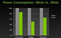
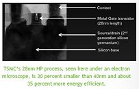
"The advancement that TSMC offered was a new optimized process technology. Kepler is manufactured using TSMC's 28nm high performance (HP) process, the foundry's most advanced 28nm process which uses their first-generation high-K metal gate (HKMG) technology and second generation SiGe (Silicon Germanium) straining," read the blog post. "Using TSMC's 28nm HP process enabled us to reduce active power by about 15 percent and leakage by about 50 percent compared to 40nm, resulting in an overall improvement in power efficiency of about 35 percent (see charts)."

TSMC Reports First Quarter EPS of NT$1.29

TSMC today announced consolidated revenue of NT$105.51 billion, net income of NT$33.47 billion, and diluted earnings per share of NT$1.29 (US$0.22 per ADR unit) for the first quarter ended March 31, 2012.

Year-over-year, first quarter revenue increased 0.1% while both net income and diluted EPS decreased 7.7%. Compared to fourth quarter of 2011, first quarter of 2012 results represent a 0.8% increase in revenue, and a 6% increase in both net income and diluted EPS. All figures were prepared in accordance with R.O.C. GAAP on a consolidated basis.

NVIDIA Licenses Integrated, OV-Tolerant I/O and ESD Tech. from Sofics and ICsense

Sofics bvba of Gistel, a leading provider of ESD solutions for ICs, and ICsense of Leuven, a prominent designer of analog, mixed-signal, and high-voltage ICs and turnkey ASICs, today announced that NVIDIA has licensed their integrated ESD and I/O technology to provide a stable 3.3V I/O with robust ESD protection on its Icera modem processors that use 1.8V transistors.

The license includes customized ESD solutions from Sofics and ICsense's overvoltage-tolerant I/Os. These solutions are based on a novel circuit technique proven in TSMC 0.18 um, 40 nm, and 28 nm processes that allows I/Os to handle more than 2X the voltage of the transistors on the chip.
Return to Keyword Browsing
Nov 22nd, 2024 22:54 EST change timezone

New Forum Posts

Popular Reviews

Controversial News Posts