News Posts matching #TSMC

Return to Keyword Browsing

NVIDIA Wants 450 mm Wafers, Seeking Foundry Partnership with GlobalFoundries, Samsung

NVIDIA is formulating a long-term chip manufacturing strategy that will see its interests secure by the time chip manufacturing has moved on to 14 nm (which follows 20 nm and today's 28 nm), which could arrive around 2015. Chip manufacturing by foundry partners is a potentially major irritant for NVIDIA, which wants to see wafer sizes getting increased from the current 300 mm manufacturing at TSMC, to 450 mm, and fast. TSMC will achieve 450 mm (18-inch) wafer manufacturing capability only by 2015. Another irritant for NVIDIA is TSMC's change in business model, which charges fabless customers "per wafer manufactured", rather than "per working chip yielded", giving them what they perceive to be the shorter end of the stick. NVIDIA is thus rigorously evaluating other foundry partners. We know from a slightly older report that Samsung has sent NVIDIA test chips manufactured at its Austin, Texas facility. There is talk that NVIDIA could also seek partnerships with GlobalFoundries, of which AMD recently relinquished all its stakes on. NVIDIA needs reliable, high-volume foundry partners that can keep it competitive not just with its main business of GPUs, but also a potential gold mine that is application processors.

NVIDIA Approaching Other Foundries than TSMC for 28 nm Production

NVIDIA, along with Qualcomm, is reportedly in talks with foundries other than TSMC, for manufacturing of its new 28 nm chips. Despite the fact that TSMC is ramping up its 28 nm capacity at a breakneck pace, NVIDIA is seeing a shortage of production that could affect its competitiveness. An interesting revelation here is that NVIDIA has begun sampling its GPUs on Samsung's 28 nanometer fab process. Samsung uses this process for contract-manufacturing of ARM application processors. Other foundries with proven 28 nm manufacturing capability include UMC.

TSMC 28 nm Capacity Ramp-Up Faster Than Older Processes

With launches of new-generation GPUs by NVIDIA and AMD, and new ARM application processor designs by various industry players, TSMC is under pressure to ramp up its production capacity for its new 28 nanometer note. DigiTimes research suggests that this ramp-up is going at a faster rate than older processes such as 40 nm and 65 nm nodes (when those were new). Digitimes Research analyst Nobunaga Chai claims that the 28 nm node started generating revenues in Q4, 2011, and sales ratio reached 5% in the following quarter. It is anticipated to see TSMC significantly ramp up its 28nm production capacity later in 2012, Chai believes.

ARM Expands Processor Optimization Packs for TSMC 40 nm and 28 nm Process Variants

ARM today announced the availability of a significantly expanded lineup of ARM Processor Optimization Pack (POP) solutions for TSMC 40 nm and 28 nm process technologies targeting a range of ARM Cortex processors. At least nine new POP configurations targeting Cortex-A5, Cortex-A7, Cortex-A9 and Cortex-A15 processor cores will be released. An essential element of ARM's comprehensive implementation strategy, POPs enable ARM partners to quickly close timing of single-, dual- and quad-core implementations across a broad envelope of power, performance and area optimization points. This solution reduces risk and improves time-to-market in the development of Cortex processor-based Systems-on-Chip (SoCs) with partners achieving competitive results in as little as six weeks.

At the leading-edge 28 nm HPM (high performance for mobile) and 28 nm HP (high performance) process variants, ARM is launching new POPs for the Cortex-A9 core as well as the first POPs for ARM's newest Cortex-A7 and Cortex-A15 processors. Since the Cortex-A7 and Cortex-A15 cores are used in tandem as ARM's big.LITTLE energy-efficient processing solution, the addition of POPs for both cores assures a complete solution for big.LITTLE implementations. ARM's lead licensee for the Cortex-A15 POP for TSMC 28 nm HPM is progressing toward the tape out of its first chip in the coming months.

TSMC Faces Acute 28 nm Capacity Shortage

Taiwan's premier semiconductor foundry, TSMC, is reportedly facing an acute shortage in 28 nm manufacturing capacity. This shortage is expected to relax in Q3, 2012, according to sources. Qualcomm, AMD, and NVIDIA are the three biggest patrons of the 28 nm process, Qualcomm uses it to manufacture performance ARM application processors, while AMD and NVIDIA use it for their new generation GPUs. Although launched at the very end of Q4 2011, AMD's HD 7970 shipped a relatively small volume due to low manufacturing capacity. NVIDIA launched only two 28 nm GPUs, the GTX 680, and GT 640M, and has had to delay launch of more models, due to this reason, according to source. Qualcomm, meanwhile, shifted some of its orders to UMC.

EVGA GeForce GTX 680 Pictured, Too, $499 Pricing Confirmed

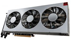
Here is the first picture of EVGA GeForce GTX 680. The best-selling GeForce AIC partner in the US, EVGA, opted for a minimalist sticker design, while sticking to NVIDIA reference board and cooler designs. In fact, all GeForce GTX 680 launched in the first-wave, do. Speaking of first-wave, TechnoReviews managed to screengrab American Retailer Newegg.com listing out nearly all the GeForce GTX 680 models that will be available on launch of the SKU.

The listing confirms the US $499 (before taxes) pricing of NVIDIA GeForce GTX 680, because that's how low these cards are available for; they will never price it below NVIDIA-recommended MSRP. Newegg.com applying a $10 margin is quite natural, they've done it with pretty much every major graphics card market-launch this year, including that of the Radeon HD 7900 series. Assuming the GeForce GTX 680 beats Radeon HD 7970, as NVIDIA claims, our educated guess is it still won't start a "price-war" as such. AMD might recalibrate prices of HD 7900 series down 5~10%, but AMD and NVIDIA won't be able to drive prices below a threshold, and that threshold is governed by TSMC, its ability to ship 28 nm chips in volumes big enough, and at prices low enough, to support a price-war between the two GPU giants.

TSMC Expanding 28 nm Manufacturing Facility

With the advent of highly-complex 28 nm discrete PC graphics processors, and ARM designers lined up with their increasingly powerful SoCs, TSMC is bound to see a pile up of orders for chips built on its newest bulk manufacturing process. In view of this, the "messiah of the fabless" is planning an expansion of its 28 nm manufacturing facility. This expansion is set to occur a little later in 2012. TSMC reportedly is running at full capacity at its 12-inch fabs because of strong demand for 28 nm as well as 40 nm and 65 nm. Due to this, some designers are approaching TSMC's competitors UMC and Samsung for 28 nm bulk manufacturing, according to sources. The expansion will follow a revision of TSMC's capex target for 2012, up from US $6 billion.

TSMC seeing orders fill sub-40nm capacity

Taiwan's premier chip foundry, TSMC, is reportedly seeing strong demand for sub-40 nm chip manufacturing. It's easy to manufacture smaller, simpler chips on new foundry nodes than complex devices such as GPUs. Hence, the source notes that it's wireless communication device chip manufactures that have sub-40 nm nodes at TSMC fully booked up. The foundly also scored orders from local and foreign fabless audio IC firms. "In fact, TSMC's 6-inch fab dedicated to process analog and LCD driver ICs has been running at full capacity since late February, with shipment delivery times to customers being extended to more than 12 weeks, the sources pointed out," notes DigiTimes.

NVIDIA Kepler Yields Lower Than Expected.

NVIDIA seems to be playing the blame game according to a article over at Xbit. This is what they had to say, "Chief executive officer of NVIDIA Corp. said that besides continuously increasing capital expenditures that the company ran into in the recent months will be accompanied by lower than expected gross margins in the forthcoming quarter. The company blames low yields of the next-generation code-named Kepler graphics chips that are made at TSMC's 28nm node. "Decline [of gross margin] in Q1 is expected to be due to the hard disk drive shortage continuing, as well as a shortage of 28nm wafers. We are ramping our Kepler generation very hard, and we could use more wafers. The gross margin decline is contributed almost entirely to the yields of 28nm being lower than expected. That is, I guess, unsurprising at this point," said Jen-Hsun Huang, chief executive officer of NVIDIA, during a conference call with financial analysts.

NVIDIA's operating expenses have been increasing for about a year now: from $329.6 million in Q1 FY2012 to $367.7 million in Q4 FY2012 and expects OpEx to be around $383 million in the ongoing Q1 FY2013. At the same time, the company expects its gross margins in Q1 FY2013 to decline below 50% for the first time in many quarters to 49.2%. Nvidia has very high expectations for its Kepler generation of graphics processing units (GPUs). The company claims that it had signed contracts to supply mobile versions of GeForce "Kepler" chips with every single PC OEM in the world. In fact, NVIDIA says Kepler is the best graphics processor ever designed by the company. [With Kepler, we] won design wins at virtually every single PC OEM in the world. So, this is probably the best GPU we have ever built and the performance and power efficiency is surely the best that we have ever created," said Mr. Huang.

Radeon HD 7700 Series Specifications Surface

In the coming week, AMD will release its Radeon HD 7700 series, which aims to increase its competitiveness in the sub-$200 market. The latest specifications exposé reveals AMD's new design strategy: Instead of increasing components such as stream processors and ROPs, which would increase transistor counts, and unnecessarily increase power draw, AMD is counting on a lesser number of better-configured Graphics CoreNext stream processors. While the previous-generation HD 5770/6770 "Juniper" GPU featured VLIW5 stream processors, the new "Cape Verde" GPU, which will go into making up Radeon HD 7770 and 7750, will feature GCN stream processors. Apart from architectural performance improvements, AMD is counting on increased clock speeds to do the trick. The specifications are listed below.

Cape Verde Physical
  • Built on TSMC 28 nm process, ~1.5 billion transistors
  • 10 Graphics CoreNext Compute Units (CUs)
  • 640 stream processors
  • 40 TMUs, 16 ROPs
  • 128-bit wide GDDR5 memory interface

IBM Contract-Manufacturing Trinity APUs for AMD

In a significant development, AMD reportedly disclosed at the Financial Analyst Day event that it has begun manufacturing its "Trinity" accelerated processing units (APUs) at IBM's foundries. With the creation of Global Foundries, AMD went fabless, relying on Global Foundries (its former manufacturing division) and the likes of TSMC to manufacture its products. Till date, Global Foundries has handled manufacture of most of AMD's CPU products, and socket FM1 APUs, while BGA APUs and chipset have been manufactured at TSMC.

What makes AMD's partnership with IBM for manufacturing a significant development is the fact that IBM can handle high-volume production, and has a proven track-record with semiconductor manufacturing process R&D, it also holds a wide range of silicon fabrication IP, rivaled only by Intel. Chips manufactured at IBM will only add to the volumes created by Global Foundries, Big Blue won't completely replace it as AMD's foundry partner. The ability to ship in greater volumes plays a significant role in scoring design wins, apart from pure performance of the product. For example, Lenovo would want to be absolutely sure you can ship in large quantities before designing a major product around your chip.

28 nm struggles: TSMC & GlobalFoundries

Making silicon chips is not easy, requiring hugely expensive fabs, with massive clean-room environments and at every process shrink, the complexity and difficulty of making the things goes up significantly. It looks like TSMC and GlobalFoundries are both having serious yield problems with their 28 nm process nodes, according to Mike Bryant, technology analyst at Future Horizons and this is causing a rash of non-working wafers - to the point of having nothing working with some chip designs submitted for production. It seems that the root cause of these problems are to do with the pressures of bringing products to market, rather than an inherent problem with the technology; it just takes time that they haven't got to iron out the kinks and they're getting stuck: "Foundries have come under pressure to release cell libraries too early - which end up with designs that don't work," Bryant said. In an effort to try and be seen to treat every customer equally, TSMC is attempting to launch ten 28 nm designs from seven companies, but it's not working out too well: "At 45-nm, only NVIDIA was affected. At 28-nm any problems for TSMC will be problems for many customers" said Bryant.

TSMC Reports Fourth Quarter EPS of NT$1.22

TSMC today announced consolidated revenue of NT$104.71 billion, net income of NT$31.58 billion, and diluted earnings per share of NT$1.22 (US$0.20 per ADR unit) for the fourth quarter ended December 31, 2011.

Year-over-year, fourth quarter revenue decreased 4.9% while both net income and diluted EPS decreased 22.5%. Compared to third quarter of 2011, fourth quarter of 2011 results represent a 1.7% decrease in revenue, and a 3.9% increase in both net income and diluted EPS. All figures were prepared in accordance with R.O.C. GAAP on a consolidated basis.

In US dollars, fourth quarter revenue decreased 5.4% from the previous quarter and decreased 4.5% year-over-year. Gross margin for the quarter was 44.7%, operating margin was 31.4%, and net margin was 30.2%.

AMD Denies Hidden GCN CUs in Tahiti

Over the past few days, we were hearing rumors from many quarters that AMD's "Tahiti" high-performance GPU may have been a deviation from an older specification, and that it really has 2304 stream processors spread across 40 GCN compute units (CUs), instead of the 32 the Radeon HD 7970 ended up with. Both AMD and NVIDIA create more redundant components on their chips than their SKUs end up getting, so they could increase yields, it's a process commonly known as "harvesting".

On Tuesday, AMD quashed the rumor in an e-mail to Bright Side of News, in which it said that Tahiti XT (Radeon HD 7970) makes use of all the CUs there are, on the chip. The 40 CU / 2308 SP rumor gained some weight with the fact that since AMD is venturing into unknown territory (TSMC's 28 nm process, built after quite some delays and failures), it could do some heavy harvesting. Examples of harvesting in recent past include Intel Sandy Bridge-E Core i7 processors, which use only up to 6 out of 8 cores on the silicon, and only up to 15 MB out of 20 MB available on it; and GeForce GTX 480, which used only 480 out of 512 CUDA cores available on the GF100 GPU.

Taiwan Foundries Cut Prices

Taiwan foundries are going to be cutting prices by 10 to 15% for wafers built on mature node processes. Since these wafers have lower production costs the foundries are passing on the savings. This move is to boost consumer confidence in building their inventory after a year of shaky ground in the U.S. and European markets. This according to DigiTimes.

Also DigiTimes is reporting despite slow demand for mature process manufacturing, Taiwan Semiconductor Manufacturing Company (TSMC) continues to see orders heat up for advanced 28nm technology, according to sources at non Taiwan-based chip suppliers.

This news could mean that these same vendors that are getting a cut in overhead thanks to the foundries could pass on the savings to the end customer to boost revenue.

TSMC 18-inch Wafer Volume Production On Course for 2015

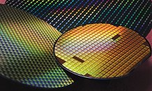
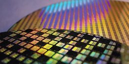
TSMC told industry observers that its plans to test large 18 inch wafers are on schedule for 2012-13, and should reach volume production in 2015. Silicon chips are manufactured on large discs known as wafers, and cut out of them. Like pizza, the sizes of wafers are measured by their diameters. The 18 inch diameter wafer has been something TSMC has been working on. Larger the wafer, the more chips can be cut out of a single wafer. It works to reduce production costs. TSMC expects to have 95% of its 18 inch wafer production equipment installed in 2014, and commence volume production by 2015. Currently, TSMC faces technical hurdles that have to be solved in collaboration with equipment and material suppliers.

AMD Radeon HD 7900 Key Features Listed

We've already been through the specifications of HD 7970 "Tahiti" in some detail that matters to those who can draw a performance hunch looking at them. This latest slide shows you the feature-set this GPU comes with. To begin with, there are three main categories of feature updates: Graphics CoreNext, AMD Eyefinity 2.0, and AMD APP Acceleration. AMD claims CoreNext to be a "revolutionary" new architecture that changes the way the GPU crunches numbers.

For the past five generations (since Radeon HD 2000), AMD GPUs have used the VLIW (very-long instruction word) core arrangement. Even the latest VLIW4 introduced by Radeon HD 6900 series, was an evolution, than a revolution of that. CoreNext replaces VLIW stream processors with super-scalar Graphics Compute cores. This should translate to higher performance per mm² die-area, resulting in smaller GPUs, giving AMD room for greater cost-cutting if the competition from NVIDIA for this generation takes effect. The GPU itself is built on TSMC's new 28 nm silicon fabrication process. Next up, AMD confirmed support for PCI-Express 3.0 interface, that nearly doubles system bus bandwidth over the previous generation.

AMD Starts Shipping 28 nm GPUs for Revenue

AMD CEO Rory Read, speaking at the IT Supply Chain conference organized by Raymond James this Tuesday, said that his company had begun shipping 28 nm GPUs for revenue (meaning, in volumes big enough to fetch revenue). With it, AMD fulfilled its promise to be the first to the market with GPUs built on the 28 nm silicon fab process. AMD's foundry partner for these chips is TSMC. "We are ramping 28nm [products] with TSMC in Taiwan and shipping the products here and now. We are very excited about the products," said Read.

At the upcoming CES event, AMD will formally unveil a range of products that will use its 28 nm GPUs. CES will give AMD a good opportunity to bag design wins with large volume manufacturers of notebooks and PCs. What this means for the enthusiast community is that whenever AMD does launch its Radeon HD 7900 series, it won't be a "paper-launch".

GeForce Kepler 104 and 100 GPU Specifications Compiled

A quick stroll through our previous article about how the GeForce Kepler family of next-generation GPUs is laid out, would tell you that GeForce Kepler 104 (GK104), is going to be NVIDIA's answer to AMD's Tahiti. GK104 will be a high-performance (≠ high-end) GPU by NVIDIA that will have many of the features that were reserved for its previous high-end GPUs (such as a 384-bit wide GDDR5 memory interface), but will not be NVIDIA's most powerful GPU in the series. The throne will be kept empty for GK100, which will comply with NVIDIA's "go all in" design ideology for high-end GPUs.

3DCenter.org compiled a few specifications of the GK104 and GK100. They go like this:
GK104
  • 640 to 768 CUDA cores
  • 80 to 96 TMUs (depending on what the CUDA core count ends up being)
  • 384-bit GDDR5 memory interface, 48 ROPs
  • Built on the 28 nm TSMC process
  • Products based on this will launch in the first quarter of 2012

AMD Tahiti GPU Specifications Compiled

If the word on the optical fibers is true, we are less than a month away from the launch of AMD's next high-end graphics card family based on its next high-performance GPU, codenamed "Tahiti". According to 3DCenter, AMD will launch new graphics card models based on this GPU around January 10, 2012. It is expected that we'll learn a lot more about these GPUs, maybe even come across AIB-branded graphics cards, at the upcoming CES event.

3DCenter compiled specifications of "Tahiti", based on bits and pieces of information from various sources. The specs can be listed out as:
  • 4.50 billion transistors, die-area of 380 mm², built on TSMC 28 nm process
  • Advanced GCN 1D architecture
  • 2048 1D processing cores
  • 128 TMUs, 48 ROPs
  • 384-bit wide GDDR5 memory interface, memory clock slightly below 1 GHz, target bandwidth of 240~264 GB/s
In Gandhi's words, salt is as free as the air.

NVIDIA GeForce Kepler Roadmap Compiled

2012-13 promises to be a period of big graphics product launches, centric to a new DirectX version, DirectX 11.1, which will ship with Microsoft's next major Windows version (currently referred to as Windows 8). Information compiled by ExpertsPC.com and 4Gamer.net tables what NVIDIA's next-generation graphics family could look like, and around what time it could be released to market. With its next-generation GeForce Kepler family of GPUs, NVIDIA will follow a sensible bottom-up product release model, to ensure that it isn't met with any technical hurdles with TSMC's new 28 nm manufacturing process, and so it could launch GPUs with increasingly higher transistor counts, till its top-of-the-line GPU is outed.

The first GPU in NVIDIA's pipeline is the GeForce Kepler 107 (GK107), on which will be based entry thru lower-mainstream SKUs. The data doesn't reveal things like core counts, but points out that GK107 will have a 128-bit wide GDDR5 memory interface, will use the current-generation PCI-Express 2.0 bus, will be built on the 28 nm process, and will support DirectX 11.1. This will be followed by the GK106, on which "sweet-spot" SKUs could be based. This will be NVIDIA's first PCI-Express 3.0 compliant GPU, it will have a 256-bit wide GDDR5 memory interface.

Are Improving Integrated Graphics Slowly Killing Off Discrete Graphics Cards?

Intel started the trend of improving integrated graphics with their second generation LGA1155 socket Core i3, i5 & i7 line of processors. Depending on the model, these processors sport integrated HD2000 or HD3000 graphics right on the processor die, which nowadays give acceptable performance for low-end gaming and can play Full HD 1080p video perfectly. This trend is increasing with the upcoming Ivy Bridge processors, which will be able to support a massive 4096 x 4096 pixel display, as we reported here. AMD now also have equivalent products with their Llano-based A-series processors. So, where does this leave discrete graphics cards? Well, the low end market is certainly seeing reduced sales, as there really isn't enough of a performance difference nowadays to always warrant an upgrade from an IGP. As integrated graphics improve further, one can see how this will hurt sales of higher end graphics cards too. The problem is that the bulk of the profit comes not from the top-end powerhouse graphics cards, but from the low to mid-end cards which allow these companies to remain in business, so cannibalizing sales of these products to integrated graphics could make high-end graphics cards a much more niche product and crucially, much more expensive with to boot.

TSMC 28 nm Technology in Volume Production

TSMC today announced that its 28nm process is in volume production and production wafers have been shipped to customers. TSMC leads the foundry segment to achieve volume production at 28nm node.

TSMC's 28nm process offering includes 28nm High Performance (28HP), 28nm High Performance Low Power (28HPL), 28nm Low Power (28LP), and 28nm High Performance Mobile Computing (28HPM). Among these technology offerings, 28HP, 28HPL and 28LP are all in volume production and 28HPM will be ready for production by the end of this year. The production-version design collateral of 28HPM has been distributed to most mobile computing customers for their product-design use.

AMD to Turn to TSMC for ''Bulldozer'' Manufacturing

AMD is rumored to be seeking ties with TSMC, Taiwan's premier semiconductor manufacturing foundry, for future manufacturing of its "Bulldozer" architecture processors, according to a report by DonanimHaber. This has two very distinct implications: first, AMD could be facing issues with GlobalFoundries 32 nm HKMG node, its de facto foundry for CPU manufacturing, and second, this could just be an obvious development of future low-power APUs based on the new x86 architecture being manufactured at TSMC, much like how current E-series and C-series APUs are.

Then again, AMD doesn't exactly have any APUs in works that use "Bulldozer" architecture for the x86 cores, rather, its successor codenamed "Piledriver". Another couple of important things to note here are that TSMC does not have a 32 nm bulk node (it was scrapped with the transition to 28 nm bulk), and its HKMG (high-K metal gate transistor) manufacturing technology is deployed rather recently. It would be interesting to follow this development.

GeForce BETA Driver Hints At First GeForce 600 Series Models

If not mission-critical stability, GeForce BETA drivers do tend to be great speculation starters. The driver information file packs entries for existing supported GPUs, as well as some future GPUs. GeForce 285 BETA drivers seem to have contained entries for two such future GPUs, marked "NVIDIA GeForce 610M" and "NVIDIA GeForce GT 630M", with identifications of NVIDIA_DEV.1058.01 and NVIDIA_DEV.0DE9.01, respectively.

These new "discoveries" more or less fall in line with an earlier report of NVIDIA having taped out its first GeForce Kepler family GPU, the GK107. It is becoming clear that NVIDIA has charted out a bottom-up course for its next GPU family, to play safe with the new 28 nm fabrication processes at TSMC, that of beginning with the simplest GPUs, and then scaling them up till the highest-performing part is perfected.
Return to Keyword Browsing
Nov 26th, 2024 15:11 EST change timezone

New Forum Posts

Popular Reviews

Controversial News Posts