News Posts matching #TSMC
Return to Keyword Browsing
Graphics major NVIDIA has begun sampling the first GPUs of its next-generation Kepler family. Kepler succeeds the present generation Fermi family of GPUs, that make up the GeForce 400 and 500 series. Members of the GeForce Kepler family will follow the codename nomenclature of GK1xx, like GeForce Fermi followed GF1xx. The first GPU being sampled is codenamed GK107. The codename suggests that this isn't the top-end part, it's more like a lower-mainstream or value segment offering.
It is reported that GK107 has a 128-bit GDDR5 memory bus, which also supports inexpensive DDR3 memory. It is built in small quantities on TSMC's 28 nanometer fab process (as the foundry isn't ready for 28 nm bulk manufacturing. NVIDIA will follow a "bottom-to-top" strategy, when dealing with a new fab process technology. It will first design the smallest, simplest GPUs in the lineup, and then gradually move on to larger ones. The first GK107-based SKUs will succeed the GeForce GT 500M series. NVIDIA will carve out four SKUs, internally, NVIDIA will refer to those as N13P-LP, N13P-GS, N13P-GT and N13E-GE, with N13E-GE being the "enthusiast" part. Its market SKU will likely succeed the GeForce GT 560M.
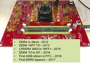
AMD showed off its first graphics processor (GPU) built on TSMC's cutting-edge 28 nanometer silicon fabrication process, the next foundry process standard for discrete GPUs. Bulk manufacturing at TSMC's Fab 15 facility at 28 nm is still taking shape, TSMC will take volume orders only later this year. For the moment, it can run small batches for designers to test their designs. The GPU was running on a mobile platform (pictured below, the red PCB), cooled by a compact copper-channel air cooler, leading us to believe that this is a mainstream segment GPU, if not lower. The demo platform was showcased running DirectX 11 title Dirt 3. Besides that, absolutely no other details were shared, not even a company codename for the GPU board.
AMD's next generation of graphics processors (GPUs) that will be branded under the HD 7000 series, are reported to be PCI-Express Generation 3 compliant. The desktop discrete graphics cards will feature PCI-Express 3.0 x16 bus interfaces, and will be fully backwards-compatible with older versions of the bus, including Gen 1 and Gen 2. Motherboards sold today feature Gen 2 PCI-E slots, although some of the very latest motherboards launched by major vendors feature PCI-Express 3.0 slots.
The new bus doubles the bandwidth over PCI-E 2.0, with 1 GB/s of bandwidth per lane, per direction. PCI-Express 3.0 x16 would have 32 GB/s (256 Gbps) of bandwidth at its disposal, 16 GB/s per direction. AMD's next generation of GPUs, codenamed "Southern Islands" will be built on the new 28 nm process at TSMC, and will upscale VLIW4 stream processors. Some of the first PC platforms to fully support PCI-Express 3.0 will be Intel's Sandy Bridge-E. Whether AMD's GPUs have hit a bandwidth bottleneck with PCI-E Gen 2, or is AMD trying to just be standards-compliant, is a different question altogether.
It looks like foundry issues are back to slow down the launch of NVIDIA's next generation high-end GPU, codenamed Kepler. The delay may push Kepler's launch to 2012, it was expected to launch by late 2011. The 28 nanometer silicon fabrication process at TSMC, a principal foundry partner of NVIDIA, is producing unsatisfactory yields. Add to that, Kepler's performance is lower than expected.
TSMC's 28 nm process at Fab 15 facility has already seen delays, which have even shaped AMD's designs in a big way. AMD had originally planned to design high-end VLIW4 chips on the 32 nm process at TSMC, but later decided to wait for the 28 nm process, leading to plans of 32 nm GPUs being scrapped by both GPU designers. TSMC was supposed to be in a position take orders of high-end 28 nm GPUs by Q4 2011, and was set to start pilot production for its 20nm process technology in the third quarter of 2012.
Acer has just placed an order for 80,000 pieces of AMD Z-series accelerated processing units. Based on essentially the same design as Fusion "Zacate", Z-series APUs are designed to have lower TDP and to be of higher quality, so they could be deployed in enterprise and IPC (industrial PC) environments. The AMD Z-01 is Acer's choice, this chip combines two x86-64 cores clocked at 1.00 GHz with AMD Radeon HD 6250 DirectX 11 compliant graphics, and a DDR3 memory controller. The TDP of the entire chip stands at 5.9W, it is built on the 40 nm process at TSMC.
Acer's first tablets based on AMD Z-01 will run Windows 7, since Android 3.0 (codenamed "Ice Cream Sandwich") is not going to be out any time before the end of 2011. Acer isn't the only big tablet-maker opting for AMD Z-series over Intel's Atom Pine Trail platform, MSI is also reported to be working on x86 tablets running AMD Z-series. Manufacturers are opting for Z-series over Pine Trail, because the latter has both higher price and TDP. With its relatively faster iGPU, Z-series should be able to drive graphics-intensive custom user-interfaces on tables sized up to 10.1-inches. Industry sources expect AMD to ship up to 500,000 units of the chip in the second half of 2011.
SPARKLE Computer Co., Ltd., the professional VGA card manufacturer and supplier, today debut the SPARKLE GeForce GTX 560 Graphics Cards, which are designed for mainstream users looking to build the premium PC gaming rig. Thanks to the improved 40nm core manufacturing process at TSMC, now the SPARKLE GeForce GTX 560 Graphics Cards have outstanding performance power consumption ratio than ever. Compared with previous generation products, the SPARKLE GeForce GTX 560 Graphics Cards also feature a special cooling system and a hardware power monitor circuit which deliver higher performance/Watt ratio. Tested in SPARKLE R&D lab, the SPARKLE GeForce GTX 560 Graphics Cards have the same power consumption as GeForce GTX 460 graphics card, but providing 28% more performance in today hottest games.
SPARKLE Computer Co., Ltd., the professional VGA card manufacturer and supplier, today presents The SPARKLE GeForce GTX 550 Ti Graphics Card, -- the latest product of SPARKLE GTX 500 Series. It delivers performance upgrade for mainstream DX11 gamers. Using the advanced Fermi 2.0 architecture from NVIDIA, the SPARKLE GeForce GTX 550 Ti Graphics Card upgrades core algorithms such as texture filtering and Z-axis compression over Fermi 1.0 architecture, so that the corresponding instruction operation efficiency is greatly enhanced. With 40nm manufacturing process improvements, now the SPARKLE GeForce GTX 550 Ti Graphics Card features higher core clock than GeForce GTS 450 graphics cards. With the two improvements, the Performance/Watt ratio of the SPARKLE GeForce GTX 550 Ti Graphics Card is 20% better over the GeForce GTS 450 graphics cards.
TSMC reiterated that it will be ready with a 28 nanometer manufacturing process by Q4 2011. The semiconductor company handles manufacturing of graphics processors for both AMD and NVIDIA. After the current 40 nm process, 32 nm, the next milestone process, was canceled for GPU makers to leap to 28 nm, this caused the foundry transition to the next process to take longer than usual. The current 40 nm process already seems to be saturated by GPUs with over 3 billion transistors, which are barely able to maintain acceptable thermal specs without using some sort of power-load throttling mechanism.
TSMC Chairman and CEO, Morris Chang, confirmed that tape-outs will be starting as early as in Q3, and production of 28 nm chips will start in Q4. Chang expects that up to 3% of TSMC's revenues will be made from 28 nm chips by the end of the year. "We plan to have around 2% or 3% of our total revenue in the fourth quarter [to] be 28nm. The tape-outs of the 28-nanaometer will start to ramp in the second half, starting in the third quarter and then more in the fourth quarter. But the real momentum [for 28nm], we believe, will be next year," Chang said. Apart from GPUs, the 28 nm process will also benefit ARM processors, with multi-core ARM chips clocked at 3 GHz being on cards. The 28 nm bulk process will also dish out AMD's next generation accelerated processing units (APUs).
SPARKLE Computer Co., Ltd., the professional VGA card manufacturer and supplier, announced the Calibre X560 Graphics Card with Accelero cooling solution from Arctic Cooling, delivering unparalleled levels of cooling performance and gaming experience to mainstream gamers. The Calibre X560 Graphics Card adopts the Fermi 2.0 architecture which upgrades core algorithms such as texture filtering and Z-axis compression over Fermi 1.0 architecture, so that the corresponding instruction operation efficiency is greatly enhanced. At the same time, with semiconductor chip manufacturing technology improvements at TSMC, through the upgrading of core components and semiconductor manufacturing process optimization of its characteristics, still based on TSMC 40nm process in the premise, The Calibre X560 Graphics Card can run at higher frequencies. By the two improvements, the Performance/Watt ratio of the Calibre X560 Graphics Card has great increase over GeForce GTX 470 graphics cards.
NVIDIA and TSMC today celebrated the shipment of the one-billionth GeForce graphics processor designed by NVIDIA and manufactured by TSMC. Today's announcement is a testament to the popularity of GeForce graphics processors, which are recognized worldwide for exceptional performance in games, video, and nearly all forms of 3D content. Today nearly every major PC manufacturer offers systems powered by GeForce GPUs.
The partners achieved the one-billionth processor milestone in less than 12 years. This achievement reflects a shared commitment to technological excellence and a relentless pace of innovation. Through deep trust and long-term objectives, the companies have raised the bar for the ambitions and practices that have helped shape the semiconductor industry.
Come this Winter, and things will heat up once again in the graphics card industry, with GPU vendors battling it out for the crucial Holidays shopping season. While AMD did not introduce any new GPUs after completing its ATI Radeon HD 5000 series launch itinerary, it did manage to grab significant amount of sales from its graphics rival NVIDIA. For this Winter, AMD and its partners will be in a position to launch the ATI Radeon HD 6000 series graphics processors, according to DigiTimes, citing sources from graphics card vendors.
It is also said that the Radeon HD 6000 series, codenamed "Southern Islands" (members of which are codenamed after islands in the Mediterranean Sea), will be built on TSMC's 40 nm manufacturing process. AMD had originally planned to build Southern Islands on TSMC's 32 nm process, but with the foundry skipping 32 nm bulk for 28 nm which will start operations only by the end of the year, AMD redrew its plans and stuck to the now-mature (stable) 40 nm process. Perhaps AMD learned a thing or two from a wide range of teething problems that plagued the 40 nm production line.
TSMC announced consolidated revenue of NT$104.96 billion, net income of NT$40.28 billion, and diluted earnings per share of NT$1.55 (US$0.24 per ADS unit) for the second quarter ended June 30, 2010. Year-over-year, second quarter revenue increased 41.4% while net income increased 64.8% and diluted EPS increased 65%. Compared to first quarter of 2010, second quarter results represent a 13.9% increase in revenue, and a 19.7% increase in both net income and diluted EPS. All figures were prepared in accordance with R.O.C. GAAP on a consolidated basis.
Gross margin for the quarter was 49.5%, operating margin was 38.6%, and net margin was 38.4%. In the second quarter, demand for TSMC's wafers continued to be strong, and wafer shipments in all major semiconductor market segments increased from their first quarter levels. Advanced process technologies (0.13-micron and below) accounted for 72% of wafer revenues. 90-nanometer process technology accounted for 16% of wafer revenues, 65-nanometer 27%, and 40-nanometer 16% of total wafer sales.
ARM and Taiwan Semiconductor Manufacturing Company, Ltd. (TWSE: 2330, NYSE: TSM) today jointly announced a long-term agreement that provides TSMC with access to a broad range of ARM processors and enables the development of ARM physical IP across TSMC technology nodes. This agreement supports the companies' mutual customers to achieve optimized Systems-On-Chip (SoC) based on ARM processors and covers a wide range of process nodes extending down to 20nm.
The agreement provides TSMC access to optimize the implementation of ARM processors on TSMC process technologies, including ARM Cortex processor family and CoreLink interconnect fabric for AMBA protocols. It also establishes a long-term relationship with ARM for the development of physical IP, including memory products and standard cell libraries targeting the most advanced TSMC 28nm and 20nm processes.
TSMC today held a groundbreaking ceremony in Taichung's Central Taiwan Science Park for Fab 15, TSMC's third 12-inch (300mm) Gigafab and an important milestone in the company's pledge to expand investment in Taiwan.
The groundbreaking ceremony was conducted by TSMC Chairman and CEO Dr. Morris Chang. "Science Parks have played a critical role in the development of Taiwan's high-tech industry. They have also provided important support to TSMC as we grew to become a leading global semiconductor company with its roots in Taiwan," Dr. Chang said. "Over the past two decades, TSMC has flourished in the Hsinchu and Tainan science parks, and our groundbreaking for Fab 15 today sets the foundation for TSMC to reach new heights."
SPARKLE Computer Co., Ltd., the professional VGA card manufacturer and supplier, today announced the SPARKLE GeForce GTX 460 series Graphics Cards, which includes the SPARKLE GeForce GTX 460 768MB Graphics Card, the SPARKLE GeForce GTX 460 1GB OC Graphics Card and the SPARKLE GeForce GTX 460 2GB Graphics Card.
As a deadly weapon of Fermi Family, SPARKLE GeForce GTX460 series graphics cards provide the best performance price ratio, being the the world's best $200 graphics card, it brings a new level of DirectX 11 performance to mainstream PC enthusiasts and gamers around the world.
One of the first pictures of NVIDIA's upcoming GF104 graphics processor has come to light, with a Chinese source picturing a GF104 qualification sample. The sample is based on the A1 silicon. The GPU package is similar to that of the GF100, it makes use of an integrated heat-spreader (IHS) to disperse heat from the die underneath it. The package is rectangular rather than square (probably a move to reduce board footprint, translating into more compact boards) The GPU is built on TSMC's 40 nm process, and is said to have significantly lower TDP compared to the GF100. One of the first SKUs built around it is the GeForce GTX 460.
Contrary to older reports, Expreview's report suggests that the GeForce GTX 460 will have 336 CUDA cores (instead of 256), and 768 MB of memory across a 192-bit GDDR5 memory interface. Its TDP is expected to be around the 150W mark, similar to that of a GeForce GTS 250. It will target price-point slightly above the $200 mark, while other SKUs carved out of this silicon will be lesser.
With AMD's next generation of graphics processors, the company plans to, at one point, switch its GPU manufacturing from its present Taiwan-based foundry partners such as TSMC and UMC, to GlobalFoundaries, its erstwhile own manufacturing division. From 40 nm, graphics processors are expected to jump to 28 nm as the next manufacturing process standard. GlobalFoundries will be ready with a 28 nm High-K metal gate (HKMG) node for making AMD products which are now bulk-manufactured in Taiwan.
During a quarterly conference call with financial analysts, chief executive officer of AMD, Dirk Meyer said "The first intersection of our AMD GPUs and GlobalFoundries are on the 28nm. We haven't been public with respect to any timing there." GlobalFoundries is said to have two principal kinds of 28 nm nodes, the 28nm-HP (High Performance) node makes complex chips such as GPUs, game console chips, storage controllers, networking and media encoding, while the 28nm-SLP (Super Low Power) is used for less complex devices, particularly intended to be low-power, for portable devices, such as baseband, application processors, and other handheld functions. In 2011, AMD is expected to release its next-generation of GPUs in a series codenamed "Northern Islands".
TSMC, one of the world's major semiconductor foundries, said that it has resolved all issues pertaining to proper yields of chips built on the 40 nanometre node. During a company event on the 19th, Mark Liu, Senior VP of Operations, said that the quality of production on the 40 nm node is almost on par with the 65 nm one. Liu stated that the chamber matching problems that had impacted yield rates for the company's 40nm node have been resolved.
TSMC caters to graphics processor giants NVIDIA and AMD, with both having designs of 40 nm performance graphics processors with multi-billion transistor counts. AMD has been selling 40 nm GPUs made by TSMC since its previous generation ATI Radeon HD 4770, it currently makes all its Radeon HD 5000 series GPUs on the node. NVIDIA is poised to release its first billion transistor 40 nm GPU, the GF100, in its consumer GeForce brand later this quarter.
In addition to this, TSMC has just finished building a new factory at the Hsinchu Science Park (HSP), Taiwan, part of its Fab 12. The new facility will be able to commence volume production of 28 nm products as early as by Q3 2010.
NVIDIA today launched its Next Generation Tegra, the world's first processor for the mobile web, specifically designed for the high-resolution needs of tablets. Consumers have been waiting for a truly portable, high-resolution, no-compromise Internet experience. NVIDIA's new Tegra processor delivers that by combining lightning-quick browsing, streaming 1080p video and Adobe Flash Player 10.1 acceleration with an immersive 3D user interface and days of battery life.
"Without question, 2010 is going to be year of the tablet," said Tim Bajarin, President, Creative Strategies, Inc. "The new NVIDIA Tegra processor has a unique feature set critical for tablets -- fast web browsing with fully rendered pages, uncompromised graphics, snappy user interface and HD video - all with the battery life we've only seen with cell phones."
NVIDIA's upcoming flagship graphics processor is going by a lot of codenames. While some call it the GF100, others GT300 (based on the present nomenclature), what is certain that the NVIDIA has given the architecture an internal name of "Fermi", after the Italian physicist Enrico Fermi, the inventor of the nuclear reactor. It doesn't come as a surprise, that the codename of the board itself is going to be called "reactor", according to some sources.
Based on information gathered so far about GT300/Fermi, here's what's packed into it:
- Transistor count of over 3 billion
- Built on the 40 nm TSMC process
- 512 shader processors (which NVIDIA may refer to as "CUDA cores")
- 32 cores per core cluster
- 384-bit GDDR5 memory interface
- 1 MB L1 cache memory, 768 KB L2 unified cache memory
- Up to 6 GB of total memory, 1.5 GB can be expected for the consumer graphics variant
- Half Speed IEEE 754 Double Precision floating point
- Native support for execution of C (CUDA), C++, Fortran, support for DirectCompute 11, DirectX 11, OpenGL 3.1, and OpenCL
GLOBALFOUNDRIES today announced the appointment of Jim Ballingall as vice president of marketing. In this role, Ballingall will be responsible for developing and implementing marketing solutions and strategies to support the growth of GLOBALFOUNDRIES as it aims to reshape the landscape of the foundry industry.
"The core of the GLOBALFOUNDRIES brand comprises the sum of the unique value propositions that we create, promise, and deliver to our customers," said Jim Kupec, senior vice president of sales and marketing at GLOBALFOUNDRIES. "As we strive to deliver on our vision and become the world's first truly global foundry, Jim's proven foundry industry leadership and experience will help us develop and convey our unique value propositions to customers and stakeholders and position the company for optimal success, as we unlock our customers' potential to innovate and win."
Taiwan Semiconductor Manufacturing Company, Ltd. has become the first foundry not only to achieve 28 nm functional 64 Mb SRAM yield, but also to achieve it across all three 28 nm nodes.
"Achieving 64 Mb SRAM yield across all three 28 nm process nodes is striking. It is particularly noteworthy because this achievement demonstrates the manufacturing benefits of the gate-last approach that we developed for the two TSMC 28 nm high-k metal gate processes," explained Dr. Jack Sun, vice president, Research and Development at TSMC.
"This accomplishment underscores TSMC's process technology capability and value in 28 nm. It shows TSMC is not only able to extend conventional SiON technology to 28 nm, but is also able to deliver the right 28 nm HKMG technology at the same time," explained Dr. Mark Liu, senior vice president, Advanced Technology Business at TSMC.
TSMC and CEA-Leti, the leading French semiconductor research institute, signed an agreement today in which TSMC will join the new industrial program IMAGINE, led by CEA-Leti, on maskless lithography for IC manufacturing. Intended to operate for three years, this program allows companies to assess a maskless lithography infrastructure for IC manufacturing and use MAPPER Technology as a solution towards high throughput. It covers a global approach, including tool assessment, patterning and process integration, data handling, prototyping and cost analysis.
Sapphire today announced its Radeon HD 4730 accelerator. The new GPU surfaced along with Radeon HD 4790. Together these GPUs fill the Radeon HD 4700 series, bringing relief to the demand Radeon HD 4770 created, but is apparently unable to meet due to technical problems with the 40 nm manufacturing node of foundry partner TSMC.
The Sapphire Radeon HD 4730 uses a PCB that is pin-compatible with Radeon HD 4870, as it is based on the same RV770 core with a different configuration. The company used a simple cooler with radially-projecting aluminum fins, which it has been using on inexpensive models of the Radeon HD 4850, and HD 4830. The memory is subjected to its air-flow, while the VRM area has a heatsink of its own. The GPU has 640 stream processors enabled, with a 128-bit wide GDDR5 memory interface, holding 512 MB of memory. Sapphire cut down on the number of memory chips used, thanks to the narrower memory bus, while maintaining the memory bandwidth of similarly clocked 256-bit GDDR3. The core is clocked at 750 MHz, while the memory is at 900 MHz (3.6 GT/s effective). The outputs provided on the card are DVI-D, D-Sub, and HDMI. The card takes its power input from two 6-pin power connectors. The card uses a 3+2 phase power circuit. The Sapphire HD 4730 is expected to be priced at 80€.
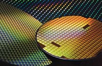
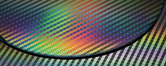
Yesterday, AMD unveiled its surprise for this year's Computex, with a demonstration of a DirectX 11 3D scene. Behind the scenes though, was what AMD claimed to be the "world's first true DirectX 11 graphics processor". The hardware itself however, wasn't publicly displayed, although a memento of AMD's partnership with TSMC, a wafer of 40 nm DirectX 11 GPUs, was made public. VR-Zone however, sneaked into the backdrops and pictured the machine that ran the demo (which ironically, was built into a case with a side-window).
The graphics card, a portion of which, is hidden behind the "wing" of the AMD Dragon logo graphic, is seen to be about 8.5 inches long, spans across two slots, and has a seemingly sporty cooler with the ATI-red shroud. It draws power from a single 6-pin PCI-E connector. The photographers note that this could be the RV840-based desktop accelerator, which forms the performance-mainstream product for the company's upcoming DirectX 11-compliant GPU lineup codenamed "Evergreen". The first product from this series is expected to be released in September, weeks ahead of the launch of Microsoft Windows 7.
Return to Keyword Browsing