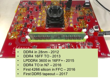
Cadence and Micron Demo DDR5-4400 Memory Module
Cadence and Micron have joined forces to build the world's first working DDR5-4400 memory module. Cadence provided their DDR5 memory controller and PHY for the prototype while Micron produced the 8 Gb chips, which were manufactured under TSMC's 7 nm process. They were able to achieve 4400 megatransfers per second, which is roughly 37.5% faster than the fastest DDR4 memory that is currently on the market. Nevertheless, Marc Greenberg from Cadence emphasized that DDR5 aims to provide increased capacity solutions, more than actual performance.
The DDR5 standard should facilitate the production of 16 Gb dies and make vertical stacking easier. Restricted by laws of physics, dies eventually get slower as they increased in size. Once you start putting 16Gb die in 1X memory technology, the distances between them starts to get longer. As a result, core timing parameters become worse. Cadence's prototype had a CAS latency of 42 (No, not a typo). Although, the test module does run at 1.1 volts, which makes it quite impressive when compared to DDR4.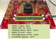

The DDR5 standard should facilitate the production of 16 Gb dies and make vertical stacking easier. Restricted by laws of physics, dies eventually get slower as they increased in size. Once you start putting 16Gb die in 1X memory technology, the distances between them starts to get longer. As a result, core timing parameters become worse. Cadence's prototype had a CAS latency of 42 (No, not a typo). Although, the test module does run at 1.1 volts, which makes it quite impressive when compared to DDR4.