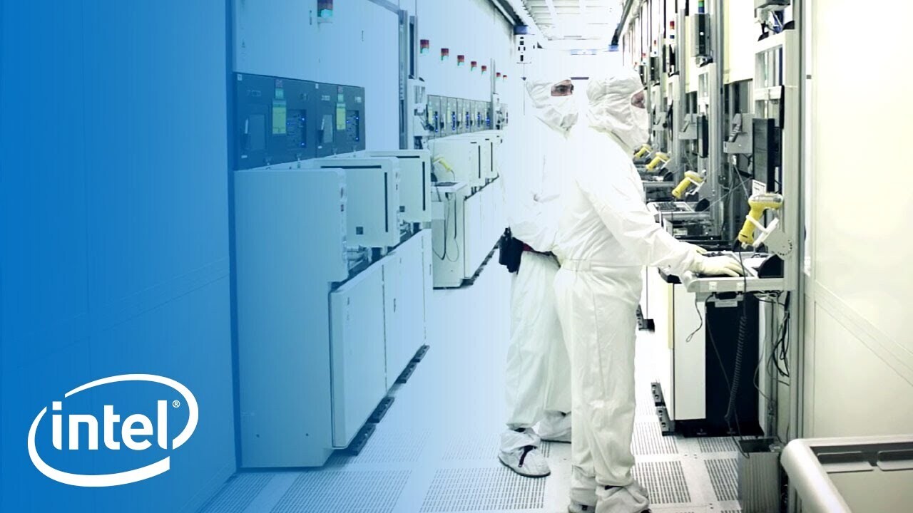
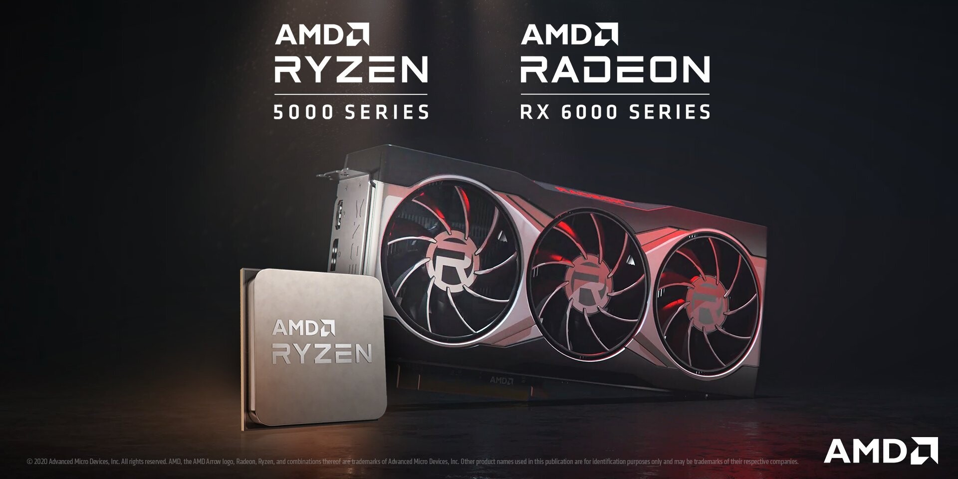
Industry Specialists Expect Chip Shortages to Last Until 2022
Industry specialists with various analysis groups have stated that they expect the world's current chip supply shortages to not only fail to be mitigated in the first half of 2021, but that they might actually last well into 2022. It's not just a matter of existing chip supply being diverted by scalpers, miners, or other secondary-market funnels; it's a matter of fundamental lack of resources and production capacity to meet demand throughout various quadrants of the semiconductor industry. With the increased demand due to COVID-19 and the overall increasingly complex design of modern chips - and increased abundance of individual chips within the same products - foundries aren't being able to scale their capacity to meet growing demand.
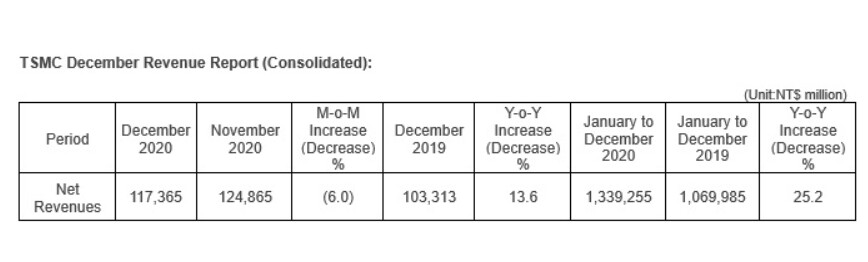
As we know, the timeframe between start and finish of a given semiconductor chip can sometimes take months. And foundries have had to extend their lead times (the time between a client placing an order and that order being fulfilled) already. This happens as a way to better plan out their capacity allocation, and due to the increased complexity of installing, testing, and putting to production increasingly complex chip designs and fabrication technologies. And analysts with J.P. Morgan and Susquehanna that are in touch with the pulse of the semiconductor industry say that current demand levels are 10% to 30% higher than those that can be satisfied by the fabrication and supply subsystems for fulfilling that demand.
As we know, the timeframe between start and finish of a given semiconductor chip can sometimes take months. And foundries have had to extend their lead times (the time between a client placing an order and that order being fulfilled) already. This happens as a way to better plan out their capacity allocation, and due to the increased complexity of installing, testing, and putting to production increasingly complex chip designs and fabrication technologies. And analysts with J.P. Morgan and Susquehanna that are in touch with the pulse of the semiconductor industry say that current demand levels are 10% to 30% higher than those that can be satisfied by the fabrication and supply subsystems for fulfilling that demand.