News Posts matching #Zen 5c

Return to Keyword Browsing

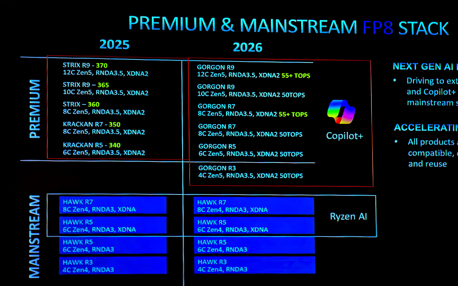
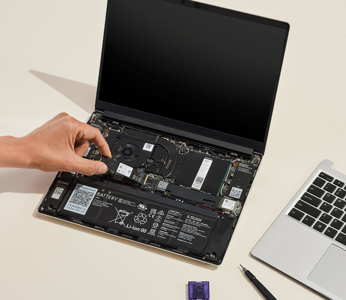
AMD Ryzen AI 9 HX 475 & 470 "Gorgon Point" APUs Surface in Shipping Manifests

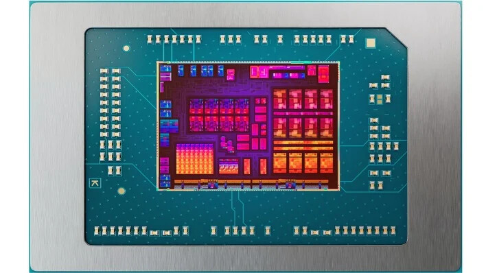
Last month, a confidential presentation in China gave AMD's laptop partners their first glimpse of what's coming next. The slides hinted at modest clock-speed improvements and the addition of more entry-level models, all under the codename "Gorgon Point." Not long after, NBD's shipping manifests today show a series of new FP8, FP10, and FP12 product codes. These identifiers don't match any existing "Strix Point" or "Kracken Point" chips, so it's clear AMD is gearing up for a Ryzen AI 400-series refresh set to roll out around mid-2026. Despite the new name, Gorgon Point sticks with the same winning formula. It still uses Zen 5 and Zen 5c CPU cores alongside RDNA 3.5 graphics and XDNA 2 neural accelerators. Core counts haven't changed, so you'll see configurations ranging from 4 to 12 cores just like before, with up to 4x Zen 5 and 8x Zen 5c cores.

What's different, according to the leaked partner slides, is a slight bump in boost clocks. The top-end Ryzen AI 9 HX 475 and 470 chips are now rated for up to 5.2 GHz, a slight but welcome increase from the previous 5.1 GHz, while maintaining a 28 W default TDP. AMD is also broadening its reach into budget laptops. In addition to the Ryzen 9 HX upgrades, the company will introduce new Ryzen 5 and Ryzen 3 models. Early leaks mention parts numbered 440 and 430, as well as a mystery Ryzen 3 SKU. These entry-level chips will use the same Gorgon Point silicon but will be tuned for cost-sensitive devices. Branding will likely follow AMD's recent pattern. Given how AMD has renumbered previous families, slotting Gorgon Point into familiar retail channels should be straightforward. Until AMD makes an official announcement, these shipping manifests and partner leaks are the best clues we have about the performance and efficiency gains in the next wave of AI-accelerated laptops.

AMD Releases AGESA ComboAM5 1.2.0.3e to Patch fTPM Vulnerability

AMD began rolling out its latest AGESA ComboAM5 microcode for Socket AM5 platforms, as confirmed by an ASUS BIOS update for its ROG Crosshair X870E Hero motherboard. The company will likely get motherboard vendors and prebuilt OEMs to release BIOS updates with the new AGESA 1.2.0.3e microcode for both AMD 600-series and AMD 800-series chipset motherboards. Version 1.2.0.3e patches a security vulnerability with the firmware TPM (fTPM) component needed to establish a hardware root of trust. This is also a minimum system requirement for Windows 11. The vulnerability discovered by Trusted Computing Group, involves an OOB (out of bounds) read method that could compromise the root of trust.

Interestingly, the ASUS change-log mentions that AGESA 1.2.0.3e introduces support for an "upcoming CPU." We know from older reports that this upcoming CPU is the Ryzen 9000G "Gorgon Point" desktop APU. These processors are based on the 4 nm "Gorgon Point" monolithic silicon, which is a revision of "Strix Point," similar to how "Hawk Point" was to "Phoenix Point." There are no changes to the IP of either the CPU complex, or the iGPU, or even the NPU, but updates to their clock speeds or boosting algorithm. The CPU consists of two CCX, one with four "Zen 5" cores sharing a 16 MB L3 cache; and the other with eight "Zen 5c" cores sharing an 8 MB L3 cache. The iGPU is based on the RDNA 3.5 graphics architecture, and comes with 16 compute units. The NPU is based on XDNA 2, and offers at least 50 AI TOPS, giving the chip Microsoft Copilot+ local acceleration capability. The PCIe complex is Gen 4, and the main PEG interface is narrowed down to PCI-Express 4.0 x8.

Sapphire at Computex 2025: Edge AI Mini PCs, NITRO+ PhantomLink Motherboard, RX 9060 XT

Sapphire brought unique new hardware to Computex 2025. We begin our tour with the new Sapphire Edge AI line of mini PCs. First up, is the Edge AI 370, a mini PC measuring 117 mm x 111 mm x 30 mm (WxDxH). It is powered by AMD Ryzen AI 9 HX 370 "Strix Point" mobile processor, with two DDR5 SO-DIMM slots supporting up to 96 GB of memory. Storage comes from a 1 TB Gen 4 NVMe SSD. The CPU is configured with 12 cores (4x Zen 5 + 8x Zen 5c), while the maxed out RDNA 3.5 iGPU has 16 CU. The XDNA 2 NPU is clocked for 50 AI TOPS, and meets Microsoft Copilot+ requirements.

Next up, is the Sapphire X870EA Wi-Fi PhantomLink Edition motherboard. This is Sapphire's first high-end motherboard in years. The Socket AM5 motherboard is based on the flagship AMD X870E chipset, and offers premium connectivity and I/O features. It's also designed to visually match the company's latest Radeon RX 9070 XT NITRO+ graphics card, but its most striking feature is PhantomLink. This is a backside power delivery feature similar to ASUS BTF. The main PCI-Express 5.0 x16 slot has a trailing power delivery slot that relays power from a 12V-2x6 power input located next to the 24-pin ATX connector on the motherboard. This may not be a complete backside I/O motherboard, but at least keeps the graphics card free from any power cables sticking out. To use PhantomLink, however, you need a compatible graphics card, and Sapphire showed us the Radeon RX 9070 XT NITRO+ PhantomLink Edition.

Two Unannounced AMD Ryzen Z2 APU Models Leaked, Flagship Could be "AI Z2 Extreme"

Three months ago, AMD unveiled its Ryzen Z2 APU series at CES 2025—purpose made for deployment in next-gen handheld gaming PCs. The officially announced flagship—Ryzen Z2 Extreme "Strix Point," utilizing Zen 5 and RDNA 3.5 technologies—was previously alluded to by leakers in late 2024; albeit with some curious claims regarding an "odd 3+5 core configuration." Last week, Hoang Anh Phu (@AnhPhuH) presented an alleged expanded lineup of Ryzen Z2 processors—headlined by a mysterious "Ryzen AI Z2 Extreme" SKU.

PC hardware watchdogs believe that this speculative variant will eventually arrive with an enabled XDNA 2 NPU (a first for the series); likely readied to take on Intel's Core Ultra 200V "Lunar Lake" processor family. MSI's Core Ultra 7 258V-powered Claw 8 AI+ and Claw 7 AI+ handhelds launched not too long ago, boasting all sorts of Microsoft Copilot+ capabilities. Mid-way through March, an Xbox executive introduced "Copilot for Gaming." Team Red and manufacturing partners are likely jumping onto this "AI gaming" bandwagon with the aforementioned "AI Ryzen Z2 Extreme" chip, as well as Phu's fanciful "Ryzen Z2 A" model. The latter could be a spin-off of AMD's vanilla Ryzen Z2 "Hawk Point" design, with a "switched on" XDNA NPU.

AMD Readies "Gorgon Point" Mobile Processor for 2026: Zen 5 + RDNA 3.5

AMD presented its next generation mobile processor that succeeds its current Ryzen AI 300 "Strix Point" to its industry partners. This presentation allegedly got leaked to the web. The 2026 successor to "Strix Point" is codenamed "Gorgon Point," and offers a significant single-threaded performance uplift while interestingly retaining the CPU core and iGPU IP. The slides mention "Gorgon Point" as combining up to 12 CPU cores based on "Zen 5" or "Zen 5c," an iGPU based on the RDNA 3.5 graphics architecture, and an NPU based on XDNA 2—so for the most part the IP is unchanged. The CPU, iGPU, and NPU, get performance upgrades over the current "Strix Point" chip.

AMD accompanied the specs slides with first party performance numbers. The multithreaded CPU performance numbers are moderately higher, which seem to indicate that the CPU core configuration of 4x "Zen 5" + 8x "Zen 5c" seems to be carried over; but the single-threaded performance sees a significant increase. We're not sure what's driving this, but there are two theories. The more obvious one is a significant increase in clock speeds, helped by an updated power management; but the second more radical theory is that AMD updated the "Zen 5" P-cores to have full fat 512-bit FP capabilities, similar to the "Zen 5" cores in "Fire Range" and "Strix Halo" processors. If you recall, the "Zen 5" cores in "Strix Point" have their FPUs limited to dual-pumped 256-bit paths to execute AVX512 instructions, a design choice probably driven by power considerations. The NPU throughput has been moderately increased to deliver over 55 AI TOPS, AMD enabled the full NPU performance across all tiers of Ryzen AI SKUs based on this chip. In all, "Gorgon Point" is to "Strix Point" what "Hawk Point" was to "Phoenix Point."

Advantech Announces Edge & AI Solutions with 5th Gen AMD EPYC Embedded Series Processors

Advantech, a leading provider of edge computing and edge AI solutions, is pleased to announce their high-performance server and network appliances are now powered by the latest AMD EPYC Embedded 9005 Series processors. By leveraging these cutting-edge platforms, Advantech is driving edge computing and AI to new heights—making solutions ideal for 5G edge cloud, AI, machine learning, and enhanced data security.

"We are excited about the launch of Advantech's latest generation of innovative edge computing and AI solutions powered by AMD EPYC Embedded 9005 Series processors," said Amey Deosthali, Senior Director of embedded core markets at AMD. "Optimized for embedded markets, EPYC Embedded 9005 provides exceptional compute performance for edge AI applications while delivering enhanced IO capabilities, product longevity, and system resiliency."

AMD Launches the EPYC Embedded 9005 "Turin" Family of Server Processors

AMD today launched the EPYC Embedded 9005 line of server processors in the embedded form-factor. These are non-socketed variants of the EPYC 9005 "Turin" server processors. The chips are intended for servers and other enterprise applications where processor replacements or upgradability are not a consideration. The EPYC Embedded 9005 "Turin" are otherwise every bit similar to the regular socketed EPYC 9005 series. These chips are based on a BGA version of the "Turin" chiplet-based processor, and powered by the "Zen 5" microarchitecture. Besides the BGA package, the EPYC Embedded 9005 series comes with a few features relevant to its form-factor and target use-cases.

To begin with, the EPYC Embedded 9005 "Turin" series comes with NTB (non-transparent bridging), a technology that enables high-performance data transfer between two processor packages across different memory domains. NTB doesn't use Infinity Fabric or even CXL, but a regular PCI-Express 5.0 x16 connection. It isn't intended to provide cache coherence, but to absorb faults across various memory domains. Next up, the series supports DRAM flush for enhanced power-loss mitigation. Upon detecting a power loss, the processor immediately dumps memory onto NVMe storage, before the machine turns off. On restart, the BIOS copies this memory dump from the NVMe SSD back to DRAM. Thirdly, the processors in the series support dual SPI flash interfaces, which enables system architects to embed lightweight operating systems directly onto a 64 MB SPI flash ROM, besides the primary SPI flash that stores the system BIOS. This lightweight OS can act like a bootloader for operating systems in other local storage devices.

Strix Point-Powered Framework Laptop 13 Introduced With Prices Starting From $899

Framework has finally introduced its next-generation Framework Laptop 13, now powered by the extremely potent Ryzen AI 300 "Strix Point" APUs. The product is already available for pre-order on Framework's website, with prices starting from $899 for the Do-It-Yourself variant, and $1,099 for the fully assembled variant. From the outside, the design of the product has been left mostly unchanged, which may appear somewhat disappointing at first, although an unaltered design likely indicates compatibility of components between the two laptops, which is undoubtedly one of the primary selling points for the Framework Laptop.

As mentioned, the biggest upgrade that the new Framework Laptop brings to the table is the new selection of processors, with the Ryzen AI 9 HX 370 APU sitting at the highest-end. Unsurprisingly, the Strix Point APUs allow for excellent performance improvements to both CPU and GPU side of things. With 12 cores (4 Zen 5 + 8 Zen 5c) and 24 threads, the highest-end Ryzen AI 9 HX 370 APU performs admirably well in benchmarks as well as real-life workloads. The Radeon 890M iGPU is among the fastest available on the market, trading blows with the Arc 140T iGPU in synthetic benchmarks. Of course, the 50 TOPS NPU allows for CoPilot functionality, for those who care. The Windows variant ships with a dedicated CoPilot key as well, while the DIY variant does not.

Acemagic Announces the Launch of the F3A AI 370 Mini PC

As a leader in innovative technology, Acemagic is excited to announce the upcoming pre-sale launch of the F3A AI 370 MINI PC by the end of January 2025. Powered by AMD's latest Ryzen AI 9 HX 370 processor, this high-performance mini PC combines outstanding computational power with cutting-edge cooling technology, designed to meet the needs of professionals, content creators, and high-end users.

The F3A AI 370 MINI PC features an advanced 12-core, 24-thread processor, built on AMD's Zen 5 and Zen 5c architecture. With a base clock speed of 2.0 GHz and a turboboost up to 5.1 GHz, it delivers exceptional multithreaded performance and processing power. Additionally, the F3A is equipped with the third-generation Ryzen AI NPU (Neural Processing Unit) based on the XDNA2 architecture, offering up to 50 TOPS of AI computing performance. With seamless collaboration between the GPU and CPU, the F3A achieves an impressive total performance of up to 80 TOPS, making it ideal for high-demand applications like deep learning and AI inference.

Beelink SER9 Pro Mini PC Gets New AMD Ryzen AI 9 365-powered Variant

The Beelink SER9 Pro made headlines a few months ago as one of the first mini PCs with AMD's Strix Point APUs. Powered by the Ryzen AI 9 HX 370 APU with the powerful Radeon 890M iGPU, the SER9 Pro promised impressive performance and efficiency in a commendably compact form factor. Now, the brand has unveiled a new variant of the SER9 Pro, powered by the slightly less-powerful Ryzen AI 9 365 APU. This variant will likely be more affordable than its higher-tier sibling, which currently starts from $999 in the US.

The differences between the Ryzen AI HX 370 and the Ryzen AI 365 are actually more substantial than one might think. Both the APUs sport four Zen 5 cores, while the AI 365 gets only six Zen 5c cores compared to the HX 370's eight. The AI 365 also gets a 100 MHz lower boost clock, and a notably slower Radeon 880M iGPU with fewer shaders. Beelink had equipped the HX 370 variant with a 65 watt TDP, but has not disclosed the TDP value for the AI 365 variant yet. That said, going by synthetic benchmark scores, the Ryzen AI 9 365 variant will likely be roughly 20% and 10% slower in CPU and GPU performance respectively than the Ryzen AI HX 370 variant.

AOKZOE A1 X Gaming Handheld Unveiled With AMD Strix Point Firepower

The market for gaming handhelds has been expanding at an unprecedented rate, largely thanks to the impressive performance and efficiency improvements brought to the table by modern APUs. AMD's Strix Point APUs are no exception, and are expected to power a multitude of high-end handhelds. Thanks to its 12 (4 Zen 5 + 8 Zen 5c) cores and RDNA 3.5-based Radeon 890M iGPU, the Ryzen AI 9 HX 370 is an impressive performer for sure. The chip can already be found in a plethora of gaming-oriented handhelds and laptops, and now a fresh offering from AOKZOE is poised to join the list.

Of course, AOKZOE is not nearly as well known as some of its competitors, such as GPD and Minisforum. AOKZOE has revealed only a single image for the product so far, and the differences between the A1, A1 Pro, and A1 X are expected to be minimal, at least on the outside. The company has revealed that the handheld will sport the aforementioned Strix Point flagship APU, along with an 8-inch display with a refresh rate of 120 Hz and a 72.7 Wh battery. These specifications are nothing extraordinary nowadays, and further details regarding the product, such as thermal performance, display quality, battery life, and the like can only be established with proper hands-on reviews. There are is no information on pricing or availability as of now, and more such details should become available as we inch closer to the A1 X's release.

AMD Expands Copilot+ Capable Ryzen AI 300 Series, Debuts Ryzen 200 Series Mainstream Mobile Processors

AMD today vastly fleshed out its mobile processor lineup with the introduction of two new processor lines besides the Ryzen AI Max 300 series. This includes the introduction of more processor models in the Ryzen AI 300 series that are powered by the "Strix Point" silicon, and the introduction of the Ryzen 200 series mobile processors, which are based on the older "Hawk Point" silicon. In 2024, AMD had debuted the Ryzen AI 300 series "Strix Point," but with just the top-end Ryzen AI 9 370 and 365, which came with maxed out 12-core/24-thread (4x Zen 5 + 8x Zen 5c) core configuration, and a maxed out iGPU with 16 CU. Today the company is introducing the Ryzen AI 7 350, the Ryzen AI 5 340, and their AMD PRO variants for commercial notebooks. Both the consumer and commercial parts have identical specs, except for the latter featuring the AMD PRO feature-set.

The Ryzen AI 7 350 comes with a CPU configuration of 8-core/16-thread (4x Zen 5 + 4x Zen 5c). All cores have a base frequency of 2.00 GHz, the Zen 5 cores boost up to 5.00 GHz. The iGPU on offer is the Radeon 860M, with 12 CU and an engine clock of up to 3.00 GHz. TDP is configurable between 15 W to 55 W. The Ryzen AI 5 340 comes with a 6-core/12-thread configuration (3x Zen 5 + 3x Zen 5c), and CPU clock speeds of 2.00 GHz base with 4.80 GHz boost achievable on the Zen 5 cores. The iGPU is heavily cut down, with just 4 CU available, and an iGPU engine clock of 2.90 GHz. Notebook designers can configure this chip with a wide power range from 15 W to 55 W. All four processor models mentioned above come with a Ryzen AI XDNA 2 NPU that's capable of 50 AI TOPS, which means they're all Microsoft Copilot+ AI PC logo eligible.

AMD Announces the Ryzen Z2 Line of SoCs for Gaming Handhelds

AMD at the 2025 International CES unveiled the Ryzen Z2 line of SoCs for gaming handhelds that combine an x86-64 based SoC with a customized version of Windows 11. This market segment is poised to heat up with the entry of the Intel Core Ultra 200V "Lunar Lake" processor, and so AMD is responding with its latest IP. The Ryzen Z2 series is based on the 4 nm "Strix Point" silicon, which combines "Zen 5" and "Zen 5c" CPU cores with a fairly large iGPU based on the new RDNA 3.5 graphics architecture that's optimized for LPDDR5X memory. AMD's engineering effort focused on modest CPU performance gains over the Ryzen Z1 "Phoenix Point," but significant graphics performance gains. The NPU is disabled on all models.

The "Strix Point" silicon physically features two CCX, one with four "Zen 5" cores sharing a 16 MB L3 cache, and the other with eight "Zen 5c" cores sharing an 8 MB L3 cache. The iGPU of "Strix Point" is based on RDNA 3.5, and comes with 16 CU (compute units), a step up from the 12 CU of "Phoenix Point." The series is led by the Ryzen Z2 Extreme, which features an 8-core/16-thread CPU configuration that probably consists of four "Zen 5" cores, four "Zen 5c" cores, and a maxed out iGPU with 16 CU. The chip has a cTDP range of 15 W to 35 W. The "Zen 5" cores boost up to 5.00 GHz.

Ryzen AI 9 HX 370-powered GMKTec EVO X1 Mini PC Goes on Sale

AMD's recently announced Strix Point APU lineup has received favorable reviews from critics and consumers alike. Especially for SFF/Mini PC enthusiasts, Strix Point brings commendable efficiency and performance to the table - both of which are absolutely essential for a high-end mini PC. The GMK EVO-X1 is surely among those, and the system is now available for purchase from GMKTec's official online store.

The EVO X1 sports a 110.19 x 107.3 x 63.2 mm chassis, which is decently compact for its class. As mentioned previously, the system is powered by the 12-core (4x Zen 5 + 8x Zen 5c) Ryzen AI 9 HX 370 APU with the shockingly potent RDNA 3.5-based Radeon 890M iGPU with 16 CUs. For most CPU-centric workloads, the EVO X1 should easily suffice. The iGPU, as mentioned, is potent enough to handle most graphically demanding tasks, including some lightweight gaming, but expecting anything more from it would be futile. Thankfully, an OCuLink port is present, which should allow for extremely fast eGPU connections courtesy of its 64 Gbps bandwidth.

OneXPlayer G1 Gaming Laptop Unveiled With Compact Enclosure and Strix Point Firepower

OneXPlayer has pulled back the veil on its G1 gaming notebook, and the product sure does look intriguing. Calling it a notebook might not even be fair, considering that its 8.8-inch display barely exceeds tablet territory. However, for lovers of compact gaming systems and handhelds, the G1 looks like it ticks many boxes, and its detachable keyboard is undoubtedly a welcome addition.

The system is powered by AMD's 12-core Ryzen AI 9 HX 370 "Strix Point" APU with 4 Zen 5 and 8 Zen 5c cores, along with a powerful Radeon 890M iGPU with 16 CUs based on the RDNA 3.5 architecture. The aforementioned 8.8-inch display is quite the looker as well, featuring a 2.5K resolution with a speedy 144 Hz refresh rate. At least on paper, it appears that the OneXPlayer G1 leaves very little room for complaint.

GEEKOM to Reveal High-performance Mini PCs at CES 2025

GEEKOM, a Taiwanese tech company famous for making high quality mini PCs, is heading to CES for the second consecutive year in 2025 with an exciting lineup of new products. Known as the Green Mini PC Global Leader, GEEKOM always focuses on improving the quality and reliability of its products, and it also spares no effort in cutting down carbon emissions and making the world a greener place.

Among the many mini PCs that GEEKOM plans to put on show at CES 2025, there are many industry firsts. The GEEKOM QS1, for instance, is the world's first mini PC powered by a Qualcomm chipset. The tiny computer sports an Arm-based Qualcomm Snapdragon X1E-80-100 processor with twelve 4.0 GHz Oryon CPU cores, a 3.8 TFLOPS Adreno X1-85 GPU and a 45 TOPS Hexagon NPU. It is smart and fast enough to breeze through all of your daily home and office computing chores, yet energy-efficient enough to significantly cut down your electric bill.

16-core AMD Ryzen AI Max+ 395 "Strix Halo" APU Outshines Ryzen 9 7945HX3D in Geekbench

Ever since AMD introduced Strix Point, enthusiasts like ourselves have been eagerly awaiting details regarding the high-end Strix Halo APUs with integrated graphics that are rumored to be powerful enough for the system to not require discrete graphics at all. Leaks regarding the upcoming performance mobile APU lineup have been trickling out steadily, and a fresh new Geekbench leak reveals the CPU performance of the Ryzen AI+ Max 395 APU, which boasts a 16-core configuration consisting entirely of Zen 5 cores, unlike Strix Point which features a mix of Zen 5 and the smaller Zen 5c cores. And oh dear, are the numbers ever so lucrative.
The APU managed to rake in 2,849 points in the single-core department, and a whopping 20,708 points in multicore. As Videocardz correctly notes, this result is far ahead of AMD's current top-end mobile offering, the Ryzen 9 7945HX3D, which manages around 16,900 points in the multicore test. In single-core, however, the Ryzen 9 7945HX3D does edge ahead, with around 2,900 points. That said, the ROG Flow Z13 laptop that the APU was housed in is most likely still in the testing phase, so it is entirely possible that the final product will sport even better performance. That being said, the Apple M4 Max SoC, however, remains in a league of its own with 3,800 points in single-core and a shocking 25,000 points in multicore. With CES 2025 just around the corner, it's only a matter of weeks before the Ryzen AI Max+ lineup finally sees the light of day and reaches our hands.

AYANEO 3 Handheld Unveiled with Hawk Point, Strix Point APUs and Optional OLED Display

AYANEO has officially revealed its latest handheld gaming console, dubbed the AYANEO 3. The company has teased the handheld multiple times in the past, while refraining from sharing any specifications regarding the same. Now, however, the company has detailed the internals for its new flagship handheld along with a few extra details.

The AYANEO 3 appears to be powered exclusively by AMD APUs, with Intel's Lunar Lake options nowhere to be found. Interested buyers will get to choose between either the Ryzen AI 9 HX 370 "Strix Point" APU, or the Ryzen 7 8840U "Hawk Point" APU. The "Strix Point" option happens to be AMD's latest and greatest, packing 4 Zen 5 and 8 Zen 5c cores, while the "Hawk Point" option sports 8 Zen 4 cores only.

AMD "Krackan / Kraken Point" APU Spotted with 4+4 CPU Core Configuration and 32 GB LPDDR5X-8000 Memory

AMD's answer to Intel's "Lunar Lake" is here. According to Olrak29, who discovered a strange entry on the OpenBenchmark benchmarking suite made by Phoronix, we have preliminary information on AMD's "Krackan / Kraken Point" APU. Spotted in the benchmark trials is the "100-000000713" model, which corresponds to an eight-core, sixteen-threaded CPU with four regular Zen 5 and four smaller (but not less potent) Zen 5c cores clocked at 3.95 GHz. Do note that this is just an engineering sample in the wild, so final clock speeds will depend mainly on AMD and its OEMs, given by TDP they plan to support with Kraken Point.

Accompanying the 8C/16T CPU configuration is the 32 GB of LPDDR5X memory from SK Hynix. According to the benchmark reading, four 8 GB modules were present, so we expect it to be on the system board, unlike on-chip like Intel does with Lunar Lake. The memory is running at 8000 MT/s, which is a 500 MT/s improvement over Strix Point and slower than its competitor, Lunar Lake, which has LPDDR5X running at 8533 MT/s. Lastly, the Krackan / Kraken Point APU has been spotted with eight RDNA 3.5 Compute Units. Where this exactly lands in AMD's product stack is still unclear. We expect to hear more about it as we enter 2025, so by then, remain patient until the next leak.

AMD Ryzen Z2 Extreme to Feature a 3+5 Core Configuration

The second generation of AMD Ryzen Z-series processors for handheld gaming consoles, will be led by the Ryzen Z2 Extreme. There will also be an affordable Ryzen Z2 (non-Extreme). We've known for some time that the Z2 Extreme is based on the 4 nm "Strix Point" monolithic silicon, with some optimization (the highest bins to facilitate the best energy efficiency); but now we have a few more details thanks to a leak by Golden Pig Upgrade. AMD's engineering effort with the Z2 Extreme will be to give the console the most generational performance uplift from the iGPU, rather than the CPU.

The "Strix Point" silicon features a significantly updated iGPU from the previous-generation "Phoenix." It's based on the more efficient RDNA 3.5 graphics architecture, which is better optimized for LPDDR5 memory; and comes with 16 compute units (CU), compared to 12 on the "Phoenix." The Ryzen Z2 Extreme will come with all 16 CU enabled. The CPU is where some interesting changes are planned. The "Strix Point" silicon features a dual-CCX CPU, one of these contains four "Zen 5" CPU cores sharing a 16 MB L3 cache, while the other features eight "Zen 5c" cores sharing an 8 MB L3 cache. For the Ryzen Z2 Extreme, AMD is going with an odd 3+5 core configuration. What this means is that the Ryzen Z2 Extreme will have 3 "Zen 5" cores, and 5 "Zen 5c" cores. The L3 cache on the CCX with "Zen 5" cores has been reduced to 8 MB in size. On paper, this is still an 8-core/16-thread CPU with 16 MB of L3 cache (same as "Phoenix,") but now you know that there's more going on.

AMD EPYC "Turin" with 192 Cores and 384 Threads Delivers Almost 40% Higher Performance Than Intel Xeon 6

AMD has unveiled its latest EPYC processors, codenamed "Turin," featuring Zen 5 and Zen 5C dense cores. Phoronix's thorough testing reveals remarkable advancements in performance, efficiency, and value. The new lineup includes the EPYC 9575F (64-core), EPYC 9755 (128-core), and EPYC 9965 (192-core) models, all showing impressive capabilities across various server and HPC workloads. In benchmarks, a dual-socket configuration of the 128-core EPYC 9755 Turin outperformed Intel's dual Xeon "Granite Rapids" 6980P setup with MRDIMM-8800 by 40% in the geometric mean of all tests. Surprisingly, even a single EPYC 9755 or EPYC 9965 matched the dual Xeon 6980P in expanded tests with regular DDR5-6400. Within AMD's lineup, the EPYC 9755 showed a 1.55x performance increase over its predecessor, the 96-core EPYC 9654 "Genoa". The EPYC 9965 surpassed the dual EPYC 9754 "Bergamo" by 45%.

These gains come with improved efficiency. While power consumption increased moderately, performance improvements resulted in better overall efficiency. For example, the EPYC 9965 used 32% more power than the EPYC 9654 but delivered 1.55x the performance. Power consumption remains competitive: the EPYC 9965 averaged 275 Watts (peak 461 Watts), the EPYC 9755 averaged 324 Watts (peak 500 Watts), while Intel's Xeon 6980P averaged 322 Watts (peak 547 Watts). AMD's pricing strategy adds to the appeal. The 192-core model is priced at $14,813, compared to Intel's 128-core CPU at $17,800. This competitive pricing, combined with superior performance per dollar and watt, has resonated with hyperscalers. Estimates suggest 50-60% of hyperscale deployments now use AMD processors.

AMD Launches 5th Gen AMD EPYC CPUs, Maintaining Leadership Performance and Features for the Modern Data Center

AMD (NASDAQ: AMD) today announced the availability of the 5th Gen AMD EPYC processors, formerly codenamed "Turin," the world's best server CPU for enterprise, AI and cloud. Using the "Zen 5" core architecture, compatible with the broadly deployed SP5 platform and offering a broad range of core counts spanning from 8 to 192, the AMD EPYC 9005 Series processors extend the record-breaking performance and energy efficiency of the previous generations with the top of stack 192 core CPU delivering up to 2.7X the performance compared to the competition.

New to the AMD EPYC 9005 Series CPUs is the 64 core AMD EPYC 9575F, tailor made for GPU powered AI solutions that need the ultimate in host CPU capabilities. Boosting up to 5 GHz, compared to the 3.8 GHz processor of the competition, it provides up to 28% faster processing needed to keep GPUs fed with data for demanding AI workloads.

AMD Readies Ryzen Z2 Chip for Handhelds Based on "Strix Point" Silicon

AMD is readying a major update to its category-defining Ryzen Z-series SoCs, with the new Ryzen Z2. Designed for handheld game consoles, the Ryzen Z-series chips are typically power-optimized variants of its mobile processors designed for ultra-low board footprint, allowing PC OEMs to build handheld game consoles with them. Facing competition from Intel's upcoming Core Ultra 200V "Lunar Lake-MX" SoCs in this segment, AMD is readying the Ryzen Z2 chip. The Z2 is based on the 4 nm "Strix Point" silicon, which gives it a significantly updated iGPU, as well as a higher core-count CPU.

Perhaps the biggest sub-system performance uplift console designers can expect from the Ryzen Z2 is graphics—AMD has given the "Strix Point" a larger iGPU with 16 compute units in place of 12 on "Phoenix," which is a 33% increase in just numerical terms. Then there's also the update to the newer RDNA 3.5 graphics architecture, which incorporates several architecture-level performance and battery-efficiency improvements. It's also better optimized for LPDDR5 memory. With CPU, AMD has given "Strix Point" a heterogeneous multicore setup with four "Zen 5" and eight "Zen 5c" cores. At this point, we don't know if all 12 cores are enabled on the Z2. ASUS is designing its next generation of ROG Ally consoles powered by the Ryzen Z2, and its designers hint that the console should be able to offer over 1 hour of "Black Myth: Wukong" gameplay on a full charge of battery—something current-gen ROG Ally X powered by the Z1 doesn't.

AMD Strix Point Silicon Pictured and Annotated

The first die shot of AMD's new 4 nm "Strix Point" mobile processor surfaced, thanks to an enthusiast on Chinese social media. "Strix Point" is a significantly larger die than "Phoenix." It measures 12.06 mm x 18.71 mm (L x W), compared to the 9.06 mm x 15.01 mm of "Phoenix." Much of this die size increase comes from the larger CPU, iGPU, and NPU. The process has been improved from TSMC N4 on "Phoenix" and its derivative "Hawk Point," to the newer TSMC N4P node.

Nemez (GPUsAreMagic) annotated the die shot in great detail. The CPU now has 12 cores spread across two CCX, one of which contains four "Zen 5" cores sharing a 16 MB L3 cache; and the other with eight "Zen 5c" cores sharing an 8 MB L3 cache. The two CCXs connect to the rest of the chip over Infinity Fabric. The rather large iGPU takes up the central region of the die. It is based on the RDNA 3.5 graphics architecture, and features 8 workgroup processors (WGPs), or 16 compute units (CU) worth 1,024 stream processors. Other key components include four render backends worth 16 ROPs, and control logic. The GPU has its own 2 MB of L2 cache that cushions transfers to the Infinity Fabric.

AMD Strix Point SoC Reintroduces Dual-CCX CPU, Other Interesting Silicon Details Revealed

Since its reveal last week, we got a slightly more technical deep-dive from AMD on its two upcoming processors—the "Strix Point" silicon powering its Ryzen AI 300 series mobile processors; and the "Granite Ridge" chiplet MCM powering its Ryzen 9000 desktop processors. We present a closer look into the "Strix Point" SoC in this article. It turns out that "Strix Point" takes a significantly different approach to heterogeneous multicore than "Phoenix 2." AMD gave us a close look at how this works. AMD built the "Strix Point" monolithic silicon on the TSMC N4P foundry node, with a die-area of around 232 mm².

The "Strix Point" silicon sees the company's Infinity Fabric interconnect as its omnipresent ether. This is a point-to-point interconnect, unlike the ringbus on some Intel processors. The main compute machinery on the "Strix Point" SoC are its two CPU compute complexes (CCX), each with a 32b (read)/16b (write) per cycle data-path to the fabric. The concept of CCX makes a comeback with "Strix Point" after nearly two generations of "Zen." The first CCX contains the chip's four full-sized "Zen 5" CPU cores, which share a 16 MB L3 cache among themselves. The second CCX contains the chip's eight "Zen 5c" cores that share a smaller 8 MB L3 cache. Each of the 12 cores has a 1 MB dedicated L2 cache.
Return to Keyword Browsing
Jul 12th, 2025 07:20 CDT change timezone

New Forum Posts

Popular Reviews

TPU on YouTube

Controversial News Posts