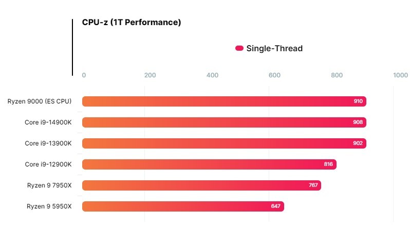
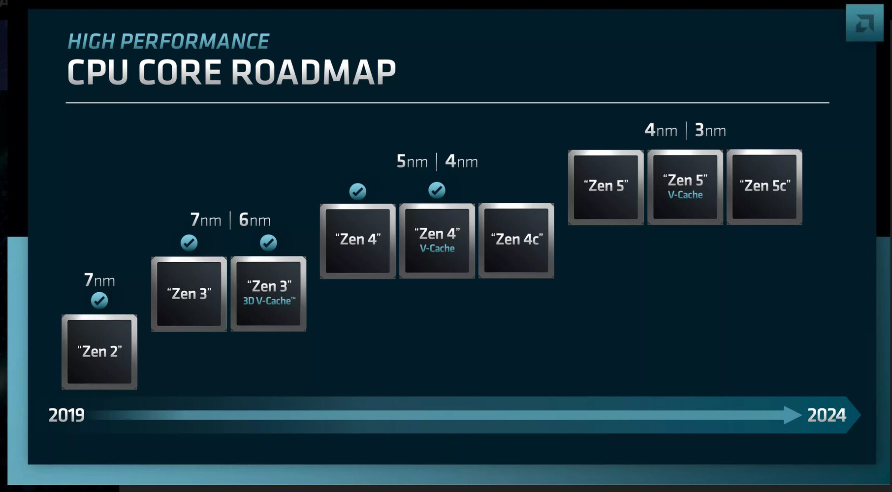
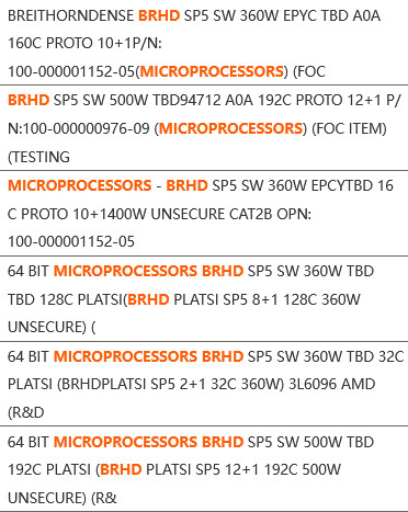
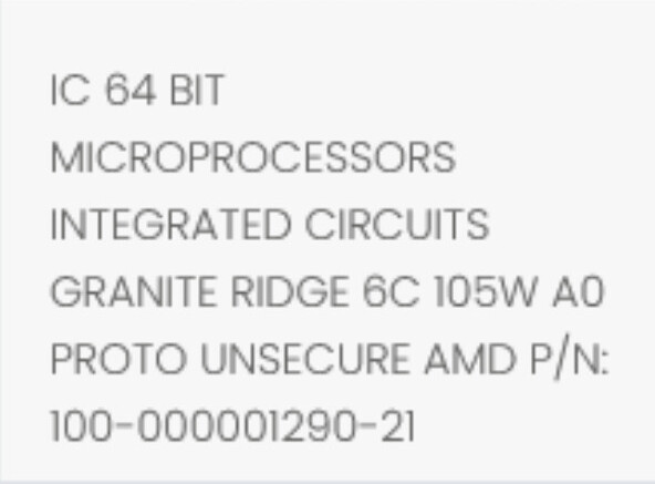
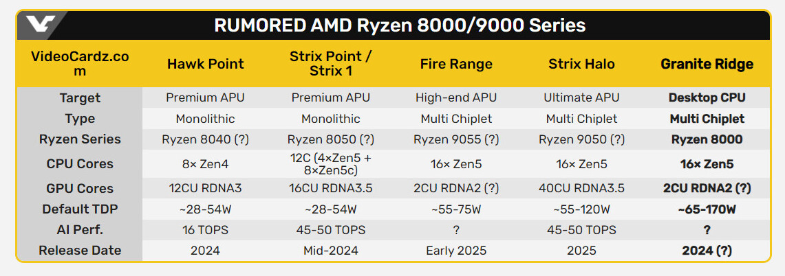
AMD Zen 5 Chiplet Built on 4 nm, "Granite Ridge" First Model Numbers Leaked
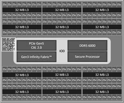
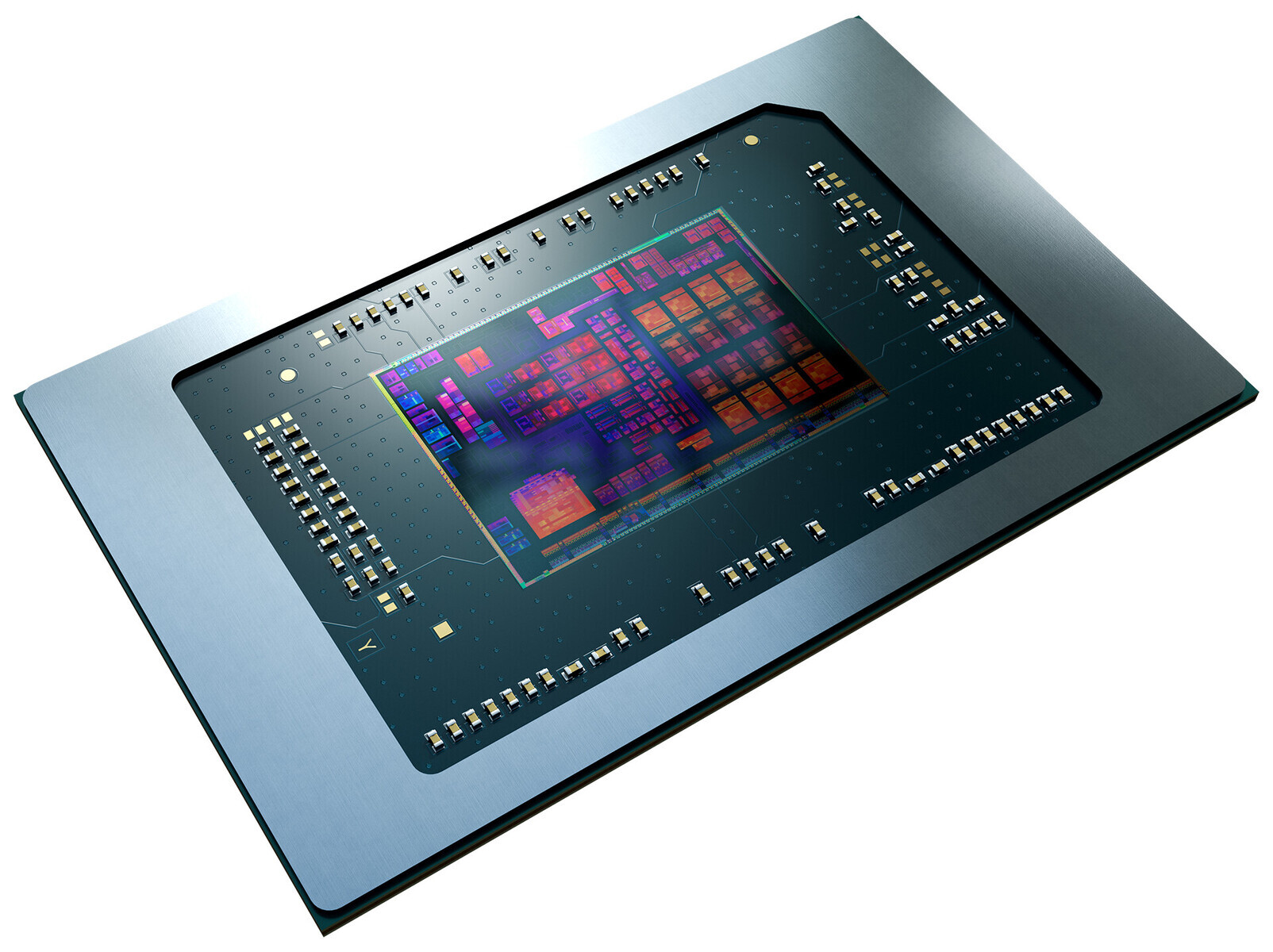
An alleged company slide by motherboard maker GIGABYTE leaked a few interesting tidbits about the upcoming AMD Ryzen 9000 "Granite Ridge" Socket AM5 desktop processor powered by the "Zen 5" microarchitecture. To begin with, we're getting our first confirmation that the "Zen 5" common CCD used on "Granite Ridge" desktop processors and future EPYC "Turin" server processors, is built on the 4 nm EUV foundry node by TSMC, an upgrade from the 5 nm EUV node that the "Zen 4" CCD is built on. This could be the same version of the TSMC N4 node that AMD had been using for its "Phoenix" and "Hawk Point" mobile processors.
AMD is likely carrying over the client I/O die (cIOD) from the "Raphael" processor. This is built on the TSMC 6 nm DUV node. It packs a basic iGPU based on RDNA 2 with 2 compute units; a dual-channel DDR5 memory controller, and a 28-lane PCIe Gen 5 root complex, besides some SoC connectivity. AMD is rumored to be increasing the native DDR5 speeds for "Granite Ridge," up from the DDR5-5200 JEDEC-standard native speed, and DDR5-6000 "sweetspot" speed of "Raphael," so the cIOD isn't entirely the same.
AMD is likely carrying over the client I/O die (cIOD) from the "Raphael" processor. This is built on the TSMC 6 nm DUV node. It packs a basic iGPU based on RDNA 2 with 2 compute units; a dual-channel DDR5 memory controller, and a 28-lane PCIe Gen 5 root complex, besides some SoC connectivity. AMD is rumored to be increasing the native DDR5 speeds for "Granite Ridge," up from the DDR5-5200 JEDEC-standard native speed, and DDR5-6000 "sweetspot" speed of "Raphael," so the cIOD isn't entirely the same.