 301
301
AMD Radeon HD 7970 3 GB Review
Packaging & Contents »Architecture
Tahiti, named after the lovely Tahiti islands of French Polynesia in the South Pacific, is AMD's new high-performance GPU. It succeeds Cayman, the chip powering the Radeon HD 6900 series and the dual-GPU HD 6990. Tahiti is built on TSMC's brand new 28 nanometer silicon fabrication process. In a nutshell, it retains the tried and trusted component hierarchy of its predecessors, but with major changes in the math processing SIMD machinery, and raster operations processors (ROPs) de-linked from the memory bus width.
With Tahiti, AMD is introducing the biggest revamp in the way its GPUs crunch numbers, since the Radeon HD 2000. Back then AMD adopted the "Graphics Parallel Core" compute architecture which uses clumps of super-scalar processors that work out "very long instruction words" (VLIW). The older version of Graphics Parallel Core used sets of four simple stream processors with one complex stream processor (that has more capabilities), along with branch units and general purpose registers. This made up with VLIW5 design. With Radeon HD 6900 "Cayman" GPU, AMD implemented a newer design that used groups of four equipotent stream processors, making up the more advanced VLIW4 design.
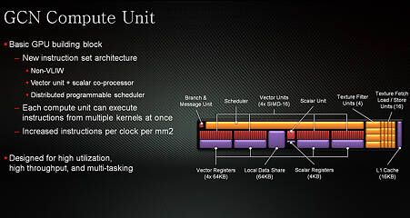
As mentioned earlier, for the most part, the GPU's component hierarchy is the same, except that its number-crunching parts have undergone, in AMD's words, a revolutionary change. VLIW5 to VLIW4 was evolutionary, in comparison. With Tahiti, AMD replaced its VLIW stream processor clusters with GCN (Graphics Core Next) compute units. Each GCN compute unit is a super-scalar processor that combines scalar and vector elements that follow a new non-VLIW instruction-set architecture, and utilizes an improved layout of shared and dedicated components. To the end-user, this architecture translates into higher performance per millimeter square of GPU die area. Smaller the GPU die, cheaper it is to produce, and sometimes, lower its power draw.
Graphics CoreNext also brings with it what AMD refers to as its 9th Generation Tessellation unit. Tahiti packs two geometry engines, and with it, two independent tessellation units. These units take advantage of larger parameter caches, new off-chip buffering capabilities, and new vertex reuse instructions to deliver a whopping four times tessellation performance improvement over the previous generation, at least on paper.
In a nutshell, the Tahiti die measures 365 mm², holding 4.31 billion transistors. It is built on the 28 nm TSMC process. It has 32 GCN compute units and 2048 stream processors in all. There are 128 texture memory units (TMUs), and 32 raster operation processors (ROPs). Despite having a 384-bit wide memory interface, the raster operations processor (ROP) count didn't increase proportionately to 48, as expected. This is because AMD reconfigured the way ROPs interact with the rest of the GPU, and hence retained its conventional ROP count of 32. The 384-bit wide memory interface combined with 5.5 GT/s GDDR5 memory chips sums up to a 264 GB/s memory bandwidth. Since it uses twelve 2 Gbit memory chips, it ends up with 3 GB of total memory on board.
Jul 10th, 2025 02:49 CDT
change timezone
Latest GPU Drivers
New Forum Posts
- Do you still use Antivirus software on your latest hardware? (75)
- Screen burn-in (21)
- TPU's Nostalgic Hardware Club (20493)
- 3DMARK "LEGENDARY" (326)
- Post Your TIMESPY, PCMARK10 & FIRESTRIKE SCORES! (2019) (321)
- 5070ti overclock...what are your settings? (47)
- 'NVIDIA App' not usable offline? (1)
- G-Sync Not Working in Borderless / Window Mode - Windows 11 (5)
- [GPU-Z Test Build] New Kernel Driver, Everyone: Please Test (78)
- Friend's monitor randomly loses signal (3)
Popular Reviews
- NZXT N9 X870E Review
- NVIDIA GeForce RTX 5050 8 GB Review
- Fractal Design Epoch RGB TG Review
- Corsair FRAME 5000D RS Review
- Fractal Design Scape Review - Debut Done Right
- AMD Ryzen 7 9800X3D Review - The Best Gaming Processor
- Sapphire Radeon RX 9060 XT Pulse OC 16 GB Review - An Excellent Choice
- Upcoming Hardware Launches 2025 (Updated May 2025)
- Sapphire Radeon RX 9070 XT Nitro+ Review - Beating NVIDIA
- PowerColor ALPHYN AM10 Review
TPU on YouTube
Controversial News Posts
- Intel's Core Ultra 7 265K and 265KF CPUs Dip Below $250 (288)
- Some Intel Nova Lake CPUs Rumored to Challenge AMD's 3D V-Cache in Desktop Gaming (140)
- NVIDIA Launches GeForce RTX 5050 for Desktops and Laptops, Starts at $249 (117)
- AMD Radeon RX 9070 XT Gains 9% Performance at 1440p with Latest Driver, Beats RTX 5070 Ti (116)
- NVIDIA GeForce RTX 5080 SUPER Could Feature 24 GB Memory, Increased Power Limits (115)
- Microsoft Partners with AMD for Next-gen Xbox Hardware (105)
- Intel "Nova Lake‑S" Series: Seven SKUs, Up to 52 Cores and 150 W TDP (100)
- NVIDIA DLSS Transformer Cuts VRAM Usage by 20% (97)


