 46
46
AMD Radeon RX 5700 Review
Packaging & Contents »Architecture: Navi and RDNA

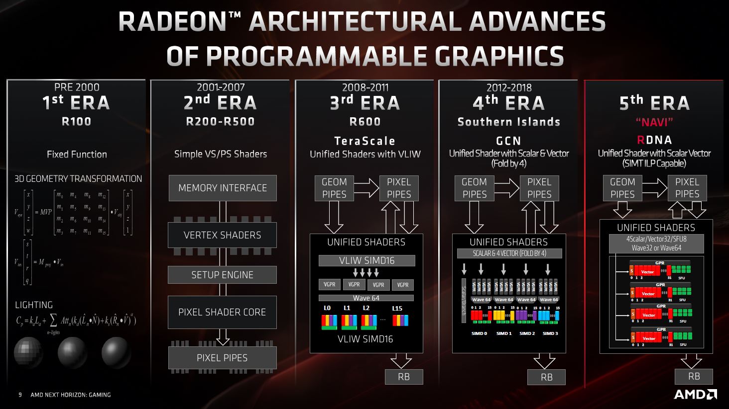
We've been hearing the moniker "Navi" for years now, and AMD threw another one at us this Computex, "RDNA", so let us demystify the two first. "Navi" is the codename for the family of silicon the GPU is based on. RDNA is a new architecture introduced by AMD to succeed Graphics Core Next (GCN). It prescribes the GPU's component hierarchy and, more importantly, its main number-crunching machinery, the compute units.
Another example of this distinction would be "Vega". Vega 10, Vega 20, and Vega 12 are pieces of silicon from the same family, while the GPU follows the 5th generation Graphics Core Next architecture governing even its compute units. Over many years, AMD made incremental updates to GCN, but this time, it claims that RDNA is sufficiently different from GCN to not be considered a new version, but rather a new hardware component that brings with it massive IPC gains over the previous generation.


The Radeon RX 5700 series is built around "Navi 10," an elegant little piece of silicon engineered on the 7 nm process at TSMC with 10.3 billion transistors crammed into a die measuring just 251 mm². The chip features a PCI-Express 4.0 x16 bus interface and a 256-bit wide GDDR6 memory interface. Infinity Fabric, which debuted on AMD's Ryzen CPUs, is extensively used as an on-die interconnect linking the various major components.
The bulk of AMD's engineering effort with RDNA has been to increase the number of dedicated resources to avoid starvation by fewer components waiting for access to a resource. The "Navi 10" silicon has two Shader Engines sharing a centralized Command Processor that distributes workloads, a Geometry Processor, and ACEs (asynchronous compute engines).


Each Shader Engine is further divided into two Graphics Engines. A graphics engine shares render backends, a Rasterizer, and a Prim Unit among five Workgroup Processors. This is where the core of RDNA begins. AMD figured it could merge two compute units (CUs) to share schedulers, scalar units, a data-share, instruction and data caches, and TMUs. The Workgroup Processor, or "dual-compute unit" as shown in the architecture block diagram, is for all intents and purposes indivisible, in that individual CUs cannot be disabled.


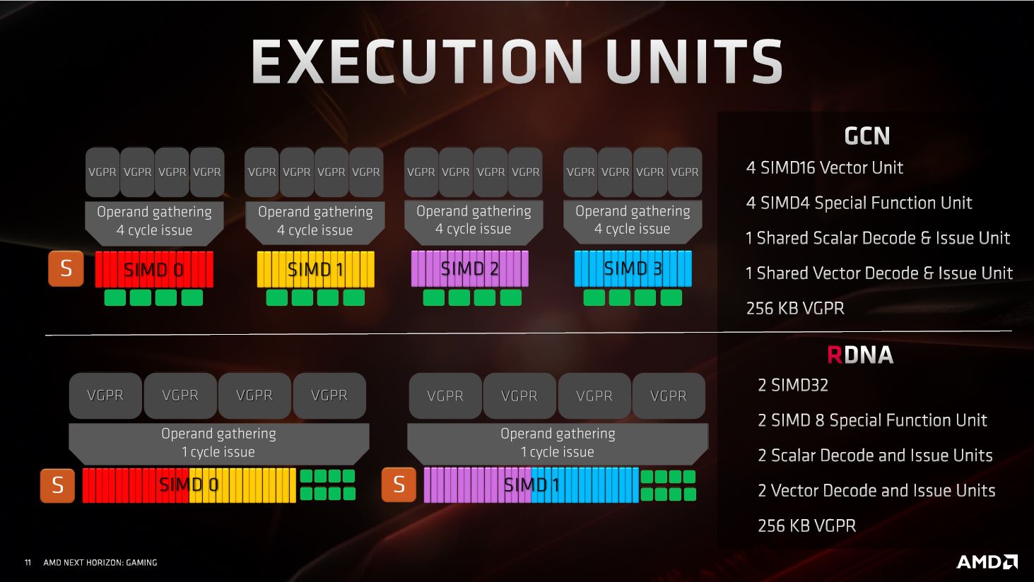
An RDNA compute unit packs 64 stream processors for vector operations and double the number of scalar units for localized serial processing. The stream processors in a CU are split into groups of two, each equipped with a scalar unit. According to AMD, this greatly reduces latency and improves the overall IPC of the compute unit. It also more efficiently utilizes local caches.


The vector execution units, or stream processors, is where much of the GPU's parallel processing happens. Due to the redesigned compute unit, two scalar processors pull two SIMD32 vector units made up of 32 stream processors, each, instead of a single scalar processor pulling four SIMD16 vector units. How is this important? On GCN, the way SIMD units are laid out, all items in a Wave64 operation get to do work once every four clocks due to hardware interleaving. With RDNA, Wave32 work items can do work every clock cycle. In all, RDNA minimizes wasted clock cycles by more efficiently and uniformly utilizing the hardware resources.


AMD examined previous generations of its graphics architecture to locate bottlenecks in the graphics pipeline. Besides increasing the number of dedicated resources, the company reworked the chip's cache hierarchy by cushioning data transfers at various stages. Each workgroup processor has dedicated 32 KB instruction and 16 KB data caches, which write back to a 128 KB L1 cache dedicated to each Graphics Engine.
These L1 caches talk to 4 MB of L2 cache. The introduction of the L1 cache and doubling in bandwidth between the various caches contributes greatly to IPC as it minimizes memory accesses, which are much slower than cache accesses. AMD is also using faster (lower latency) SRAM that reduces cache latencies by around 20 percent on die and by 8 percent at the memory level. AMD also introduced new features to the ACEs that include async-compute tunneling.

AMD summarizes the benefits of RDNA in a 25 percent IPC gain over the latest version of GCN, and an effective 50 percent performance gain for the GPU when taking into account IPC, the 7 nm process, and gains from the frequency and power management (ability to sustain boost frequencies better).


Elsewhere on the silicon, AMD updated the Display Engine and Multimedia Engine to keep up with the latest display and video standards. The Display Engine now supports DSC 1.2a (display stream compression) along with output standards HDMI 2.0 and DisplayPort 1.4 HDR to support display formats as bandwidth-intensive as 4K 240 Hz or 8K 60 Hz over a single cable, and support for 30 bits per pixel color depth. The multimedia engine supports VP9 and H.265 decoding at up to 8K 24 Hz, or 4K 90 Hz, and hardware-accelerated H.265 encoding at up to 4K 60 Hz.
Features: FidelityFX and Anti-Lag


With each new graphics architecture, gamers expect new image quality enhancement features. NVIDIA introduced DLSS, and AMD's response to that is FidelityFX, a combination of content-specific and image-specific quality enhancements. The first part of this is contrast-adaptive sharpening, which brings out details in a scene by enhancing their contrast. To work best, it requires some work from game developers, to declare which parts of the image are to be sharpened (like the HUD and on-screen texts). Details such as wear-lines on the slick tires of a race-car,or hexagonal patterns on a wall come to life. We will test this feature later in a separate article.
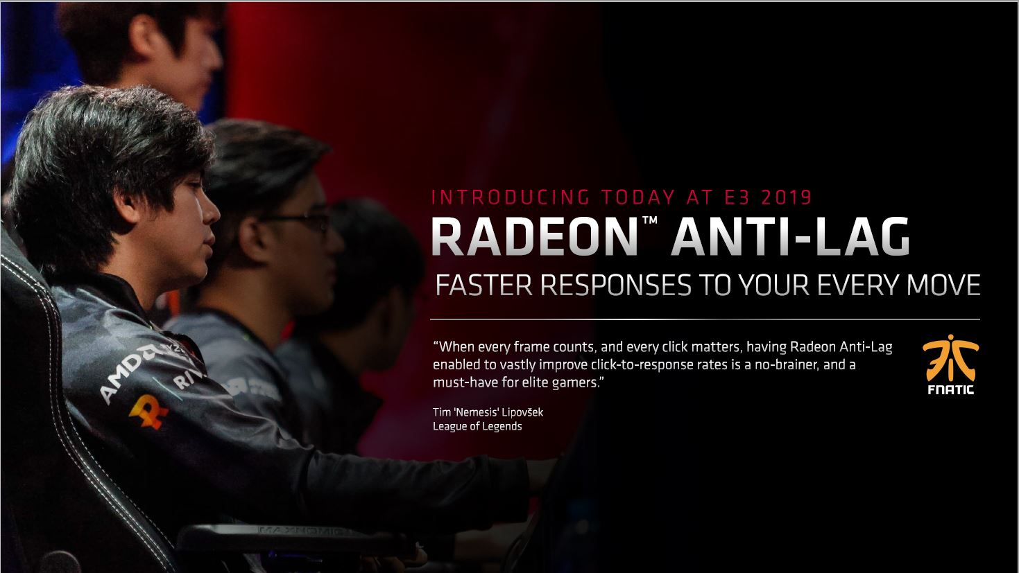


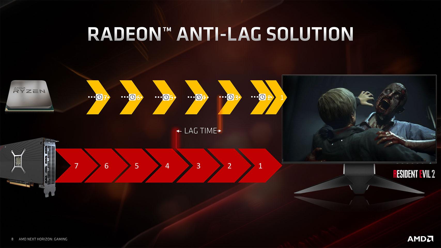
AMD wants to improve its adoption by professional e-Sports gamers by addressing a key bottleneck with modern high-end graphics: mouse-lag. This would be the amount of time taken for a click to register and a response to be rendered by the GPU. Radeon Anti-Lag is a CTR (click-to-response) enhancement that reduced mouse lag by roughly a third across various popular e-Sports titles. This setting is effectively identical to "pre-rendered" frames on NVIDIA. Modern GPUs calculate one or two frames ahead, so they can better time sending them to the monitor to avoid stuttering. Of course, this results in input lag because any input information that comes in only makes it to the screen one or two frames later.
AMD carved the RX 5700 out of the "Navi 10" silicon by randomly disabling two workgroup processors, amounting to four CUs. The resulting stream-processor count is 2,304, and 144 TMUs. The 64 ROPs and memory configuration remain unchanged.
Mar 28th, 2025 18:59 EDT
change timezone
Latest GPU Drivers
New Forum Posts
- 8 cores cpu (40)
- Future-proofing my OLED (51)
- 9070 XT - 2x HDMI high refresh displays (144 and 120 Hz) not working (72)
- Is RX 9070 VRAM temperature regular value or hotspot? (260)
- What are you playing? (23293)
- The future of RDNA on Desktop. (171)
- Undervolting help for newbie - msi vector i9 13980 hx rtx 4080 (3)
- Sexy Mechanical Keyboard Thread (507)
- The TPU UK Clubhouse (25993)
- Can you guess Which game it is? (5)
Popular Reviews
- Sapphire Radeon RX 9070 XT Pulse Review
- Samsung 9100 Pro 2 TB Review - The Best Gen 5 SSD
- Assassin's Creed Shadows Performance Benchmark Review - 30 GPUs Compared
- Pulsar Feinmann F01 Review
- ASRock Phantom Gaming B860I Lightning Wi-Fi Review
- be quiet! Pure Rock Pro 3 Black Review
- Sapphire Radeon RX 9070 XT Nitro+ Review - Beating NVIDIA
- ASRock Radeon RX 9070 XT Taichi OC Review - Excellent Cooling
- ASRock Phantom Gaming B850 Riptide Wi-Fi Review - Amazing Price/Performance
- AMD Ryzen 7 9800X3D Review - The Best Gaming Processor
Controversial News Posts
- MSI Doesn't Plan Radeon RX 9000 Series GPUs, Skips AMD RDNA 4 Generation Entirely (142)
- Microsoft Introduces Copilot for Gaming (123)
- AMD Radeon RX 9070 XT Reportedly Outperforms RTX 5080 Through Undervolting (118)
- NVIDIA Reportedly Prepares GeForce RTX 5060 and RTX 5060 Ti Unveil Tomorrow (115)
- Over 200,000 Sold Radeon RX 9070 and RX 9070 XT GPUs? AMD Says No Number was Given (100)
- NVIDIA GeForce RTX 5050, RTX 5060, and RTX 5060 Ti Specifications Leak (96)
- Retailers Anticipate Increased Radeon RX 9070 Series Prices, After Initial Shipments of "MSRP" Models (90)
- China Develops Domestic EUV Tool, ASML Monopoly in Trouble (88)