 266
266
AMD Radeon RX 9070 Series Technical Deep Dive
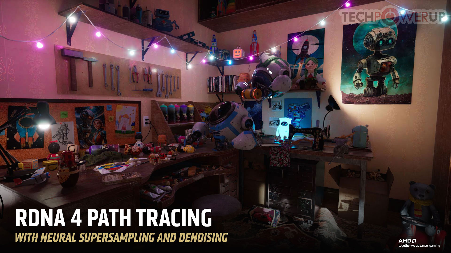
FSR 4, & AMD Software »Architecture
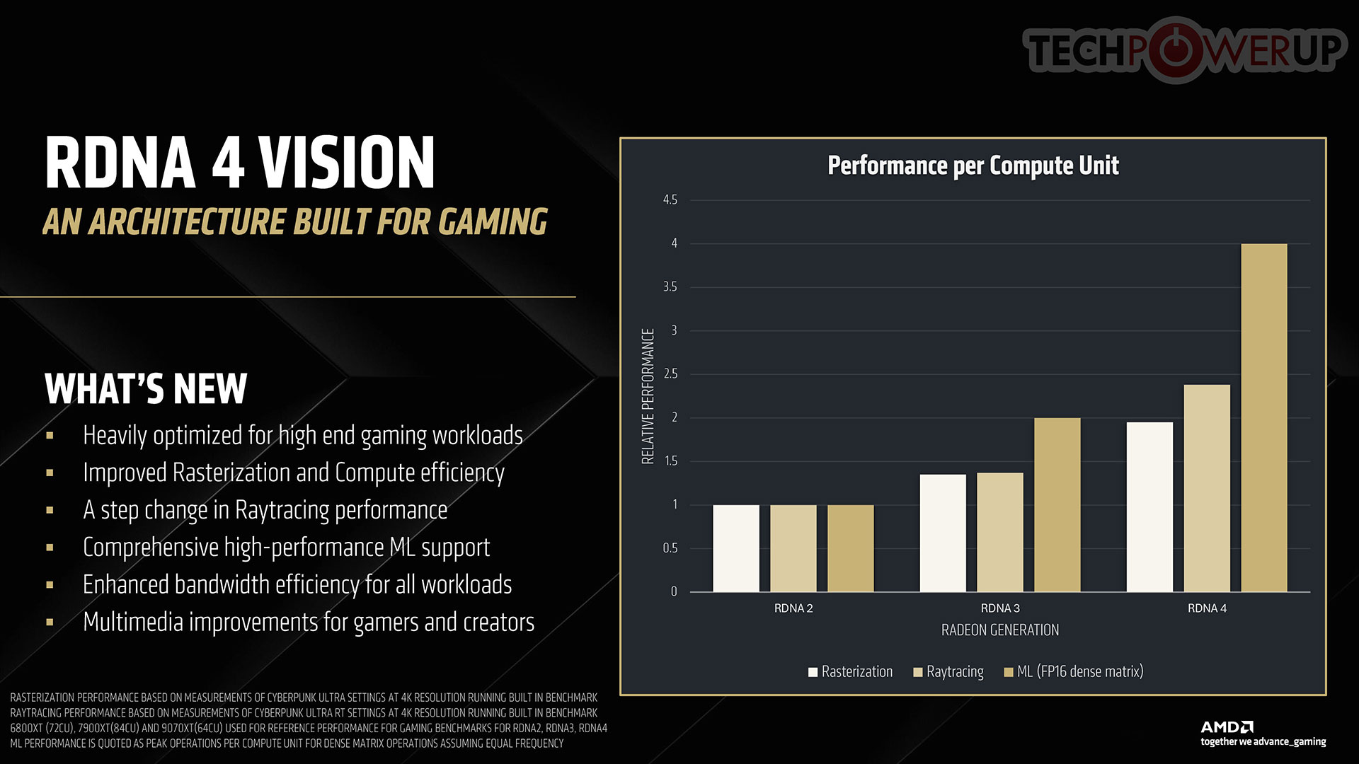
With RDNA 4, AMD looks to make GPUs that are physically smaller and hence cheaper to make, with which it can wage price-wars against NVIDIA's performance segment and mainstream SKUs, and win at any given price-point. To pull this off, the company had to ensure that it got a generational leap in performance per compute unit (CU), the indivisible number-crunching machinery of AMD GPUs.
You'll see in the slide above that the RDNA 4 CU has achieved a 100% gain in classic raster 3D performance over RDNA 2 (RX 6000 series). Kudos to AMD for not comparing this with the older RDNA 1 (RX 5000 series). RDNA 3 posted a roughly 35% gain over RDNA 2. This is big, as AMD can now lower the CU counts and make its GPU dies physically small. Next up, we see that AMD claims to have achieved an astonishing 240% gain in ray tracing performance per CU over RDNA 2, which was the company's first DirectX 12 Ultimate GPU architecture. RDNA 3 pales in comparison with only a 40% gain.
Pay attention to the last bar, which talks about machine learning acceleration (ML) performance, where AMD claims a 400% gain over RDNA 2, and 200% gain over the previous RDNA 3. This is huge, as AMD can now leverage the AI acceleration capabilities of the silicon to implement ML-based upscalers for FSR 4 that provide vast improvements in image quality at any given quality tier.
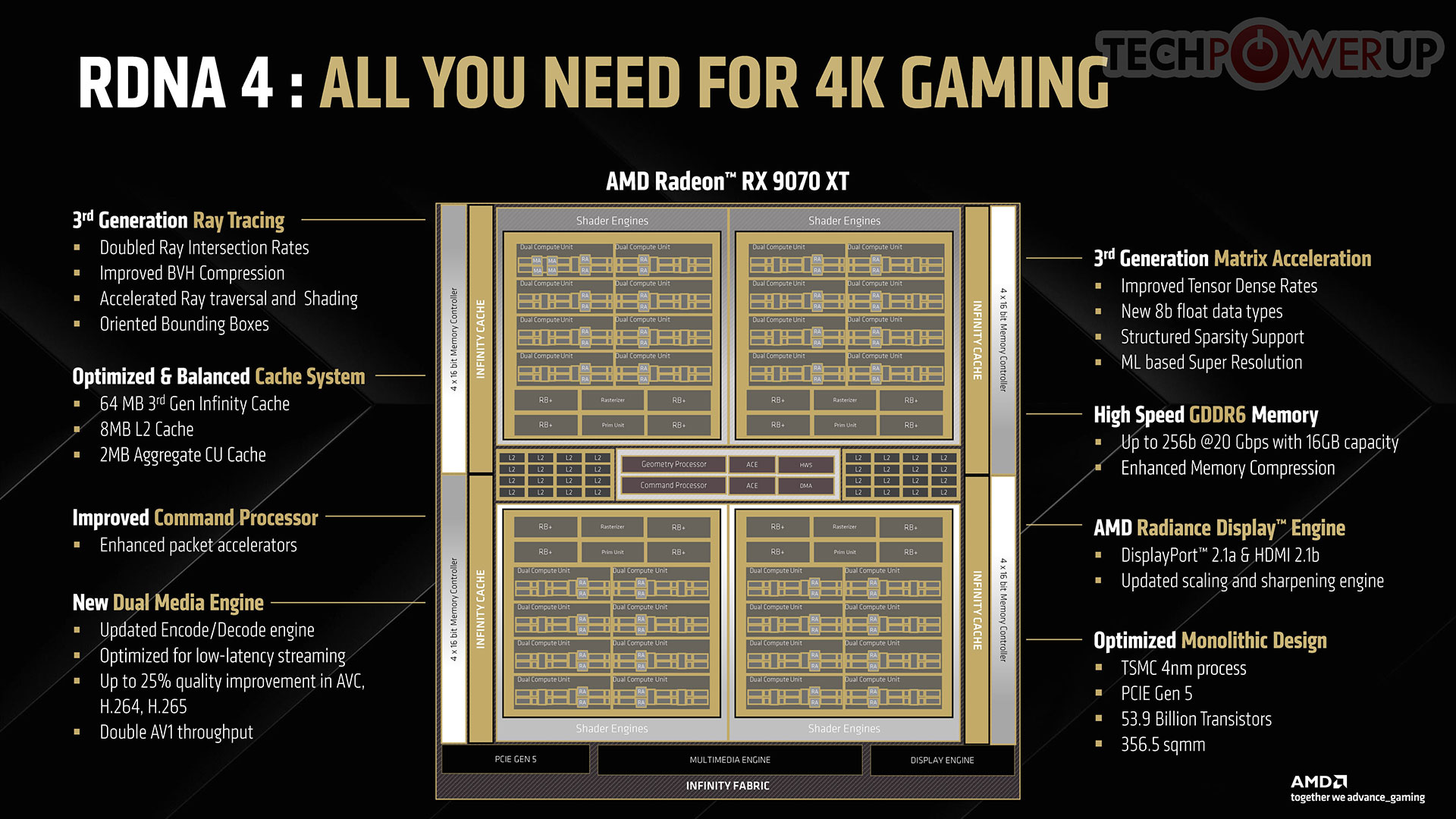
Here it is, the Navi 48 silicon powering the RX 9070 series in all its glory. The block diagram looks awfully similar to the Navi 10 powering the RX 5700 series, with its four Shader Engines. At the top level, the Navi 48 is a monolithic silicon, built on the TSMC N4C (4 nm EUV) foundry node. This is technically more advanced than the N4P node on which AMD builds many of its current-gen products.
The Navi 48 is a rectangular die. It has an area of 356.5 mm², but with an impressive transistor count of 53.9 billion. To give this number some important context, the previous "big Navi" GPU, the Navi 31 powering the RX 7900 XTX, has 57.8 billion transistors (just 8% more), despite having 96 CU, a larger Infinity Cache, and a wider 384-bit memory bus. The Navi 31 has a die area of 529 mm² (304 mm² for the 5 nm GCD, with the rest being 6 nm MCDs), so you can see the kind of strides AMD made with die-area.
At the top-level, the Navi 48 features a PCI-Express 5.0 x16 host interface, and a 256-bit wide GDDR6 memory bus. It's surprising why AMD didn't post generational gains in memory bandwidth. With 20 Gbps GDDR6 memory chips, the RX 9070 XT gets 640 GB/s of memory bandwidth. This is made up for with a faster 64 MB Infinity Cache, and a critical improvement AMD made to its memory management system, called Out-of-Order Memory Queuing, more on this later.
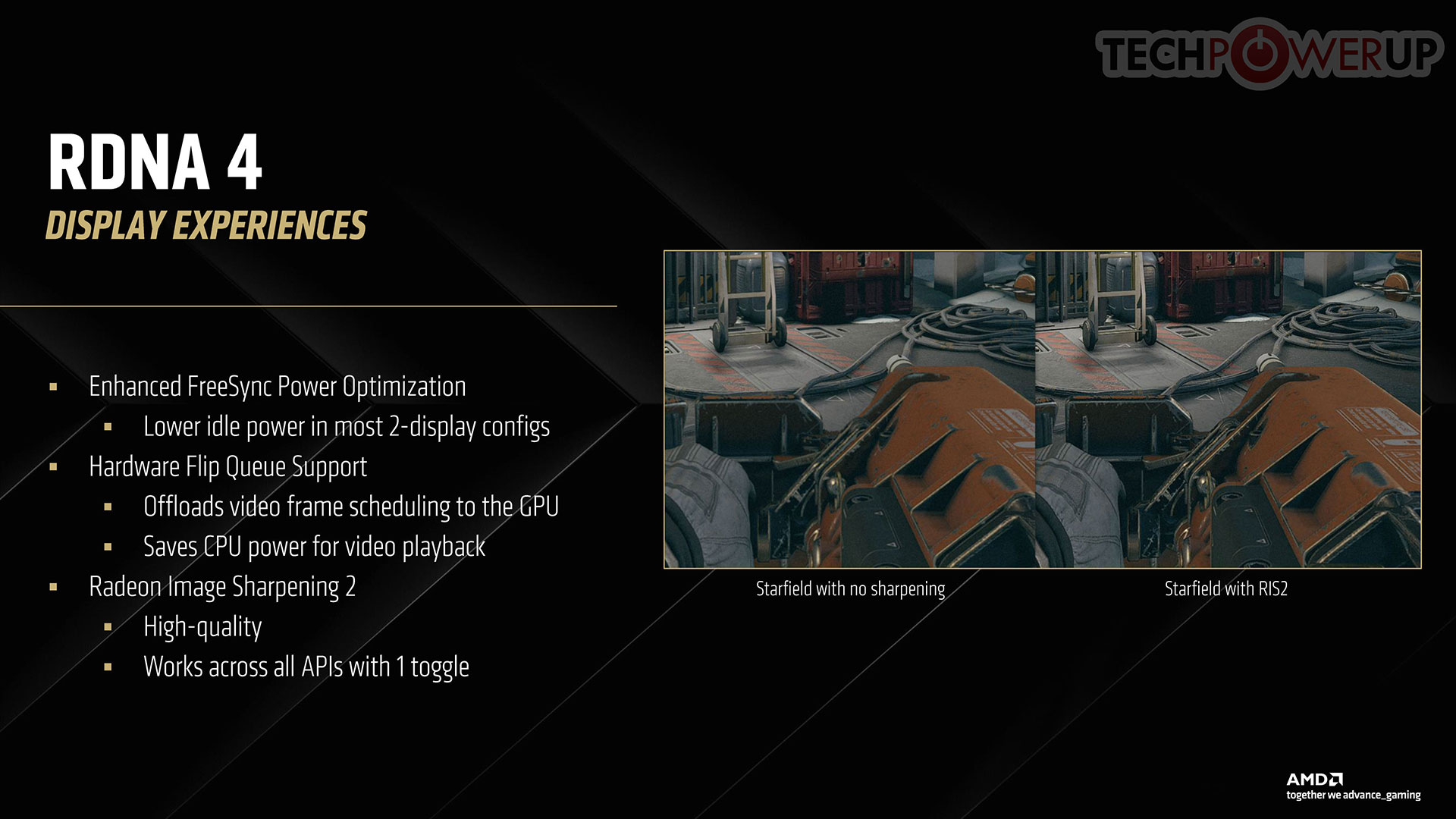
The new Radiance 2 Display Engine comes with major hardware updates that reduce GPU idle power draw in multi-monitor setups. The engine also comes with hardware flip-metering support (something NVIDIA also introduced with Blackwell, and which enables Multi-Frame Gen on the RTX 50-series). Flip-metering improves video frame pacing to the GPU and reduces CPU overhead for video playback. There is also a display engine level hardware image sharpening component that drives Radeon Image Sharpening. As for I/O, you get contemporary DisplayPort 2.1a and HDMI 2.1b, the maximum bitrate is UHBR 13.5.
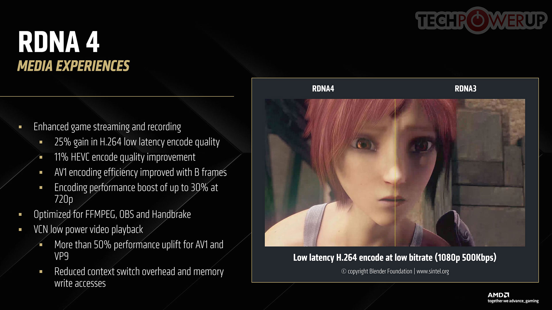
Navi 48 comes with a dual media engine, each of the two can perform concurrent encoding and decoding, and so the implementation resembles an NVIDIA GPU having two each of NVENC and NVDEC units. The new generation media engine offers a 25% increase in H.264 low-latency encode quality, and an 11% improvement in HEVC encode quality. AV1 encode and decode get B-frames support, vastly improving bitrates. A B-frame is a frame that lacks image information, but instead motion-vector values, that lets the decoder reconstruct the image component using past and future I-Frames (frames with image data). The media engine posts a 50% generational performance uplift (measured in encoder/decoder frame rates), with reductions in memory overhead.
The RDNA 4 Dual Compute Unit
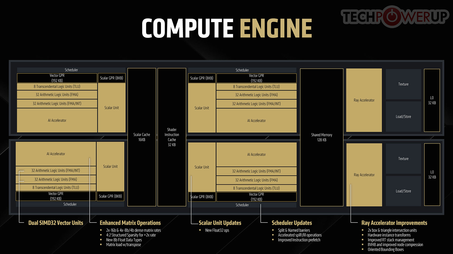
At the heart of the RDNA 4 graphics architecture is the new dual compute unit, with a vastly improved memory sub-system, improvements made to the scalar units, a new technology called dynamic register allocation, and improvements to CU efficiency and engine clocks. Each CU has two scheduler blocks, driving a 192 KB general purpose register (GPR), an 8 KB scalar GPR, 32 FMA ALUs, and 32 FMA+INT ALUs. There are also 8 transcendental logic units. RDNA 4 introduces the concept of dual SIMD32 vector units, for even more parallelism. The Scalar Unit comes with support for newer Float32 ops. Schedulers are updated with accelerated spill/fill operations. Instruction prefetching is improved.
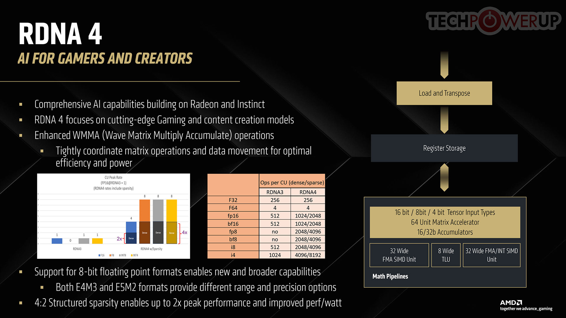
The new generation AI Accelerator comes with two 16-bit and four 8-bit/4-bit dense matrix compute rates, support for 4:2 structured sparsity for doubling throughput, and matrix loads with transpose. AMD has incorporated many technologies from its CDNA 3 Instinct AI ML accelerators on the AI Accelerators of RDNA 4, including enhanced and power-optimized WMMA, improvements to the ops per CU, support for FP8, E4M3 and E5M2 formats, and 4:2 structured sparsity.
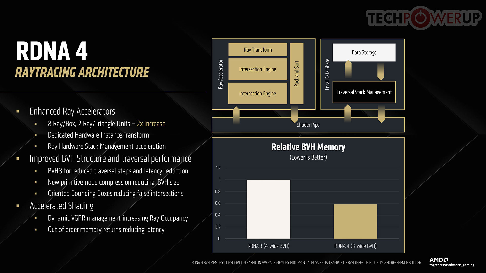
The new generation Ray Accelerator comes with double the box and triangle intersection resources as RDNA 3 RT accelerator, support for hardware instance transforms, improvements to the RT stack management, BVH8 node compression, and a revolutionary feature called oriented bounding boxes. To contain the number of rays really needed to be tested against an object, modern ray tracing technologies use something called a bounding box, which defines a region in which a geometry has to be tested against rays.
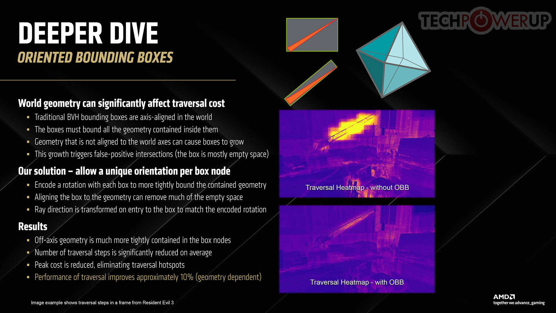
Most of the time, the geometry is of a vastly different shape and smaller than the shape of a bounding box, which introduces false intersections, and wastes ray testing resources. AMD innovated a way to turn this bounding box into a 3D shape by giving it a Z-axis component, so the bounding box is oriented closer to the shape of the object to be tested, reducing the number of rays needed to be tested against it.
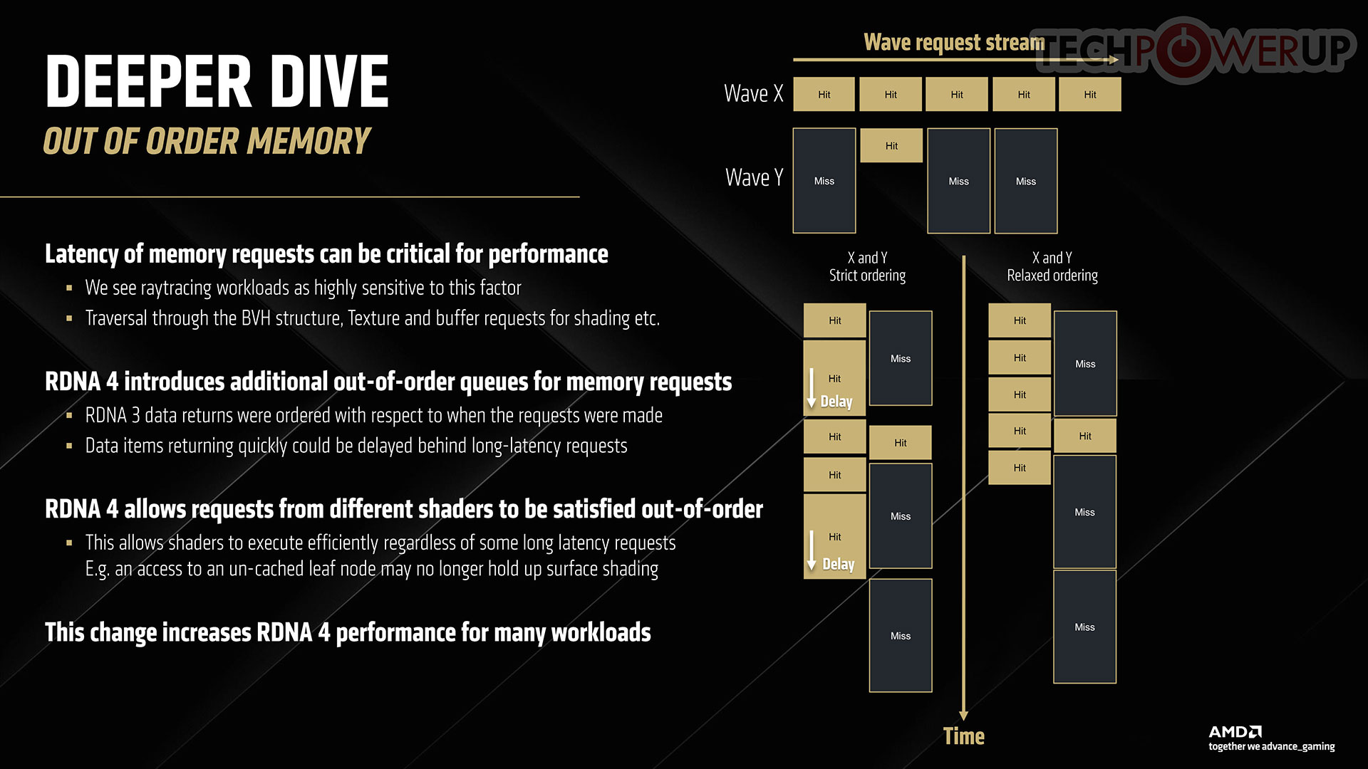
Both ray tracing and ML acceleration are memory sensitive applications, and so AMD innovated a revolutionary change to its memory management system, with the introduction of new out-of-order memory. All math is executed in waves on an RDNA GPU, and mutual dependencies between waves can cause memory request stream misses, as one wave's memory request queue waits for the other wave to complete its task. This is solved with a new out-of-order (relaxed ordering) memory management.
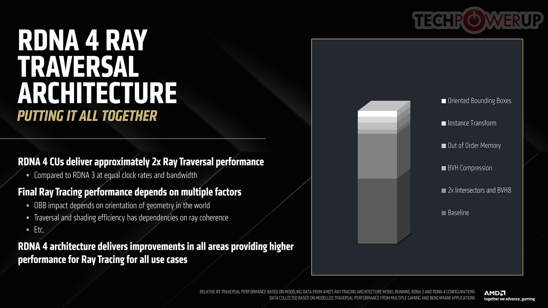
This graph highlights the contribution of various components toward the 100% generational ray traversal performance gain, allowing AMD to make do with a CU count of 64, with RDNA 3 being the baseline.
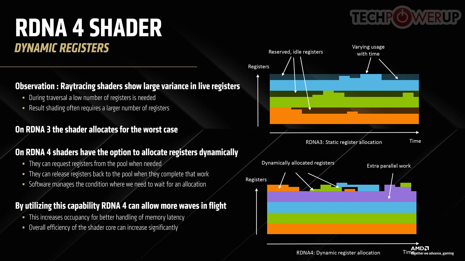
On AMD, a fairly big chunk of the ray tracing stack continues to be executed on shaders, but the company has made advances to ensure the cost of ray tracing on the shader resources of the GPU, with the introduction of Dynamic Registers, to improve parallelism.

The strides AMD made with RT accelerator performance enabled the company to make advances with path tracing, with the introduction of directed light grid sampling and neural radiance caching; restir direct and global illumination; and an ML-based pixel super sampling and denoising. That's right, AMD now uses an AI-based denoiser much like NVIDIA, which should reduce the shader performance cost of this crucial RT process.
Mar 30th, 2025 20:49 EDT
change timezone
Latest GPU Drivers
New Forum Posts
- What is the latest game you finished or 100% (7)
- Is the futureproof gaming solution a four drive system? (23)
- Folding Pie and Milestones!! (9452)
- Looking for Palit 5090 Gamerock OC BIOS (19)
- 5070 Ti power limit questions (22)
- Your PC ATM (35307)
- 13500 or 14500 or 12700 or 12700k (17)
- Regarding i7-4790k and overclocking! (11)
- What are you playing? (23323)
- Free Games Thread (4603)
Popular Reviews
- Sapphire Radeon RX 9070 XT Pulse Review
- ASRock Phantom Gaming B850 Riptide Wi-Fi Review - Amazing Price/Performance
- Samsung 9100 Pro 2 TB Review - The Best Gen 5 SSD
- Palit GeForce RTX 5070 GamingPro OC Review
- Sapphire Radeon RX 9070 XT Nitro+ Review - Beating NVIDIA
- Assassin's Creed Shadows Performance Benchmark Review - 30 GPUs Compared
- Enermax REVOLUTION D.F. 12 850 W Review
- AMD Ryzen 7 9800X3D Review - The Best Gaming Processor
- ASRock Radeon RX 9070 XT Taichi OC Review - Excellent Cooling
- XPG LEVANTE II 360 Review
Controversial News Posts
- AMD RDNA 4 and Radeon RX 9070 Series Unveiled: $549 & $599 (260)
- MSI Doesn't Plan Radeon RX 9000 Series GPUs, Skips AMD RDNA 4 Generation Entirely (142)
- Microsoft Introduces Copilot for Gaming (124)
- AMD Radeon RX 9070 XT Reportedly Outperforms RTX 5080 Through Undervolting (119)
- NVIDIA Reportedly Prepares GeForce RTX 5060 and RTX 5060 Ti Unveil Tomorrow (115)
- Over 200,000 Sold Radeon RX 9070 and RX 9070 XT GPUs? AMD Says No Number was Given (100)
- NVIDIA GeForce RTX 5050, RTX 5060, and RTX 5060 Ti Specifications Leak (96)
- Retailers Anticipate Increased Radeon RX 9070 Series Prices, After Initial Shipments of "MSRP" Models (90)