 29
29
AMD Vega Microarchitecture Technical Overview
(29 Comments) »Conclusion
AMD's Vega GPU architecture indeed heralds some of the biggest changes to GPU design from the company's stable in a while. With Vega, AMD has taken on some of the fundamental shortcomings of its GPU architectures in the area of memory management while building on its strengths in the area of compute.
Memory management has historically been AMD's architectural bane. Rival NVIDIA has been able to make do with comparatively narrower memory buses, while making use of the available bandwidth better. At least the perception that memory is bottlenecking performance was never allowed to come up for NVIDIA. AMD, on the other hand, has been throwing in brute memory bandwidth to overcome its fundamental memory management issues, and was beginning to hit a wall where throwing physical bandwidth at the problem was either getting to costly or too energy inefficient. A case in point is its 512-bit GDDR5 memory interface with "Hawaii" and the industry's first HBM implementation to take on GPUs with relatively narrower 384-bit GDDR5 memory interfaces. With Vega, AMD is addressing many of the memory management issues that have been intrinsic to its Graphics CoreNext architecture, with the introduction of its High Bandwidth Cache technology.
The company has, simultaneously, built on its architectural strengths over NVIDIA, in the areas of its compute machinery. The industry has taken a liking for the powerful and open Compute Unit design of AMD Graphics CoreNext, and with Vega, the company improved these compute units with even better instructions per clock (IPC) thanks to Rapid Packed Math, support for ISA FP16 micro-ops, which will prove big as game developers handle several of their shaders and effects as low-bandwidth FP16 ops. AMD has also revamped its rendering pipeline to be more efficient, with conservative rasterization and an improved geometry processing pipeline.
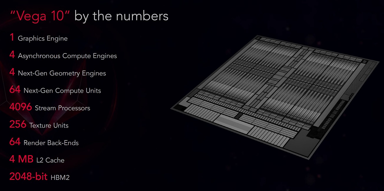
As with the "Fiji" silicon from 2015, which powered the pioneering Radeon R9 Fury series, the "Vega 10" silicon implements exotic technology like high-bandwidth memory on-package, sitting on a silicon interposer. AMD, however, does not want to be caught unprepared for a price-war with NVIDIA where it couldn't sell the R9 Fury series below a certain price. The "Vega 10" silicon has been more cleverly built. It has just two memory stacks instead of four, while retaining memory bandwidth and doubling memory capacity. The package itself is smaller.
AMD has carved out three consumer SKUs from the "Vega 10" silicon, which are priced to compete more with NVIDIA's GeForce GTX 1080 and GTX 1070 based on the company's third-biggest GP104 silicon (after the GP102 and GP100), and so for AMD marketing, it's back to the alt-left marketing strategy of giving the most for the least money and bringing the most in features to the performance segment. We only hope AMD doesn't restrict itself to this segment and builds bigger GPUs based on this otherwise technically advanced architecture.
Jul 12th, 2025 00:00 CDT
change timezone
Latest GPU Drivers
New Forum Posts
- Can you guess Which game it is? (217)
- Quick charging your USB devicesUSB 3.2 Gen 2x2 Type-C® front-panel. (1)
- NVIDIA RTX PRO 6000 Workstation Runs Much Hotter Than 5090 FE (21)
- GTX 1050 GPU Owners Club (12)
- ASUS ProArt GeForce RTX 4060 Ti OC Edition 16GB GDDR6 Gaming - nvflash64 VBIOS mismatch (2)
- Will you buy a RTX 5090? (640)
- No offense, here are some things that bother me about your understanding of fans. (33)
- What are you playing? (23919)
- Best motherboards for XP gaming (102)
- Amazon Prime days sale (3)
Popular Reviews
- Fractal Design Epoch RGB TG Review
- Corsair FRAME 5000D RS Review
- Lexar NM1090 Pro 4 TB Review
- NVIDIA GeForce RTX 5050 8 GB Review
- NZXT N9 X870E Review
- Sapphire Radeon RX 9060 XT Pulse OC 16 GB Review - An Excellent Choice
- AMD Ryzen 7 9800X3D Review - The Best Gaming Processor
- Upcoming Hardware Launches 2025 (Updated May 2025)
- Chieftec Iceberg 360 Review
- Our Visit to the Hunter Super Computer
TPU on YouTube
Controversial News Posts
- Intel's Core Ultra 7 265K and 265KF CPUs Dip Below $250 (288)
- Some Intel Nova Lake CPUs Rumored to Challenge AMD's 3D V-Cache in Desktop Gaming (140)
- AMD Radeon RX 9070 XT Gains 9% Performance at 1440p with Latest Driver, Beats RTX 5070 Ti (131)
- NVIDIA Launches GeForce RTX 5050 for Desktops and Laptops, Starts at $249 (119)
- NVIDIA GeForce RTX 5080 SUPER Could Feature 24 GB Memory, Increased Power Limits (115)
- Microsoft Partners with AMD for Next-gen Xbox Hardware (105)
- Intel "Nova Lake‑S" Series: Seven SKUs, Up to 52 Cores and 150 W TDP (100)
- NVIDIA DLSS Transformer Cuts VRAM Usage by 20% (97)