 109
109
AMD Zen 5 Technical Deep Dive
Overclocking »Zen 5 Architecture


Unlike Intel, AMD hasn't been radically changing its CPU core architecture over these past five generations of Zen, dating back to the original from 2017. Zen was designed to be highly modular, and AMD has a path to scale up the various core components, the way they connect, and their bandwidths; when combined with new foundry nodes, to succeed with double-digit percent IPC increases with each generation. The company has had consistent success with this from Zen to Zen 4, and we expect the company's IPC gain claims for Zen 5 to hold up.

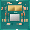
Here's a close-up picture we took of Zen 5 cores on the two CCDs of a Ryzen 9 9950X engineering sample that was on display at AMD. The CCDs are built on the TSMC 4 nm node, a slightly more advanced node than the 5 nm node that Zen 4 CCDs are built on; and we can tell that Zen 5 is a fairly big core.

AMD has made improvements across all three key regions of the core, the front-end, the execution engine, and the load/store backend. With each new generation of Zen, AMD has been improving the branch prediction unit as it contributes significantly to the generational IPC gain. With Zen 5, AMD claims to have lowered the latency around the branch prediction unit, improved prediction accuracy, and throughout toward the L1 instruction cache and op-cache. AMD has doubled decode pipes this generation.


The execution engine sees significant changes with Zen 5. To begin with, AMD broadened the dispatch retire queues to 8-wide from 6-wide. The Integer engine has 6 ALUs with 3 multiply units, an improved ALU scheduler, and a larger execution window. Perhaps the biggest change in the execution unit is the Floating Point Unit (FPU), which features a physical 512-bit FP pipe for AVX-512 with full 512-bit data path. If you recall, AMD implemented AVX-512 on Zen 4 using a dual-pumped 256-bit FPU, which at the time was seen as an energy-efficient way to do it. A 512-bit FPU should give Zen 5 a significant improvement in AVX-512 performance over Zen 4. For client processors, this should improve AI acceleration.

The Load/Store unit features a handful bandwidth improvements. To begin with, AMD increased the L1 Data cache size to 48 KB 12-way, up from 32 KB 8-way on Zen 4. The bandwidth from the FPU to the L1D cache has been doubled over Zen 4. The dedicated L2 cache remains 1 MB in size, and 16-way.

AMD proceeded to give us its measurements of IPC for Zen 5. This is a geomean of a series of single-threaded benchmarks run by AMD, comparing a Zen 5 processor to a Zen 4 processor running at identical clock speeds.


And there you have it, AMD is claiming a 16% IPC increase over Zen 4. This is measured over a series of tests mentioned in the graph above. It can range as low as +10% for a game test like Far Cry 6, and as high as 35% on Geekbench 5.4 (which uses AVX-512). Speaking of which, applications and benchmarks that utilize AVX-512 instructions should see the biggest generational performance uplifts with Zen 5, thanks to the physical 512-bit FPU replacing the dual-pumped 256-bit FPU on Zen 4. These gains range between 32% on machine learning workloads, and 35% for AES-XTS encryption (a 512-bit floating point workload).

Here's a breakdown of how improvements in each area contribute to the 16% IPC uplift. It's interesting to see the fetch and branch prediction play a smaller role compared to the execution engine, and decode/OpCache.
Zen 6 and Zen 7

In the presentation we got our first name-drop of the Zen 6 microarchitecture and its compacted Zen 6c variant. AMD does such roadmap slides to show how it's been consistently delivering on them with no delays. It's able to do this because TSMC has been keeping up its roadmap due to big ticket customers such as Apple and Qualcomm. In a discussion session we even heard an AMD spokesperson mention "Zen 7," but without any further details.
The Zen 5 and Zen 5c cores will be implemented across 4 nm and 3 nm foundry nodes. Both the Zen 5 CCDs on Granite Ridge, and the Strix Point monolithic processor are built on 4 nm, however AMD is working on high-density chipsets for 5th Gen EPYC that will see AMD implement 3 nm. Although it mentioned Zen 6 and Zen 6c, there are no foundry nodes attached to them. If we were to guess, those could ride on TSMC 2 nm and 1.8 nm. Although not on the slide, AMD also verbally mentioned Zen 7 during its presentation. So now we know that the company will continue developing Zen into its 10th market year, as Zen 7 could power AMD processors around 2027.
Jul 12th, 2025 00:30 CDT
change timezone
Latest GPU Drivers
New Forum Posts
- Can you guess Which game it is? (221)
- What are you playing? (23920)
- RX 9070 XT freezing/locking up only on desktop, anyone else? (43)
- NVIDIA RTX PRO 6000 Workstation Runs Much Hotter Than 5090 FE (22)
- Quick charging your USB devicesUSB 3.2 Gen 2x2 Type-C® front-panel. (1)
- GTX 1050 GPU Owners Club (12)
- ASUS ProArt GeForce RTX 4060 Ti OC Edition 16GB GDDR6 Gaming - nvflash64 VBIOS mismatch (2)
- Will you buy a RTX 5090? (640)
- No offense, here are some things that bother me about your understanding of fans. (33)
- Best motherboards for XP gaming (102)
Popular Reviews
- Fractal Design Epoch RGB TG Review
- Corsair FRAME 5000D RS Review
- Lexar NM1090 Pro 4 TB Review
- NVIDIA GeForce RTX 5050 8 GB Review
- NZXT N9 X870E Review
- Sapphire Radeon RX 9060 XT Pulse OC 16 GB Review - An Excellent Choice
- AMD Ryzen 7 9800X3D Review - The Best Gaming Processor
- Upcoming Hardware Launches 2025 (Updated May 2025)
- Our Visit to the Hunter Super Computer
- Chieftec Iceberg 360 Review
TPU on YouTube
Controversial News Posts
- Intel's Core Ultra 7 265K and 265KF CPUs Dip Below $250 (288)
- Some Intel Nova Lake CPUs Rumored to Challenge AMD's 3D V-Cache in Desktop Gaming (140)
- AMD Radeon RX 9070 XT Gains 9% Performance at 1440p with Latest Driver, Beats RTX 5070 Ti (131)
- NVIDIA Launches GeForce RTX 5050 for Desktops and Laptops, Starts at $249 (119)
- NVIDIA GeForce RTX 5080 SUPER Could Feature 24 GB Memory, Increased Power Limits (115)
- Microsoft Partners with AMD for Next-gen Xbox Hardware (105)
- Intel "Nova Lake‑S" Series: Seven SKUs, Up to 52 Cores and 150 W TDP (100)
- NVIDIA DLSS Transformer Cuts VRAM Usage by 20% (97)