 26
26
ASRock Fatal1ty X79 Champion Intel LGA2011 Review
BIOS Walkthrough »The Board - A Closer Look


Like any good overclocking board should, the ASRock Fatal1ty X79 Champion comes with onboard POWER and RESET switches found on the board's bottom edge. The BIOS chip, containing a 64 Mb AMI UEFI BIOS, is contained in a user-serviceable socket, a nice feature should you like to change BIOS versions but don't want to boot the machine - great for perhaps saving both a daily usage profiled BIOS and another for running extreme clocking under LN2.
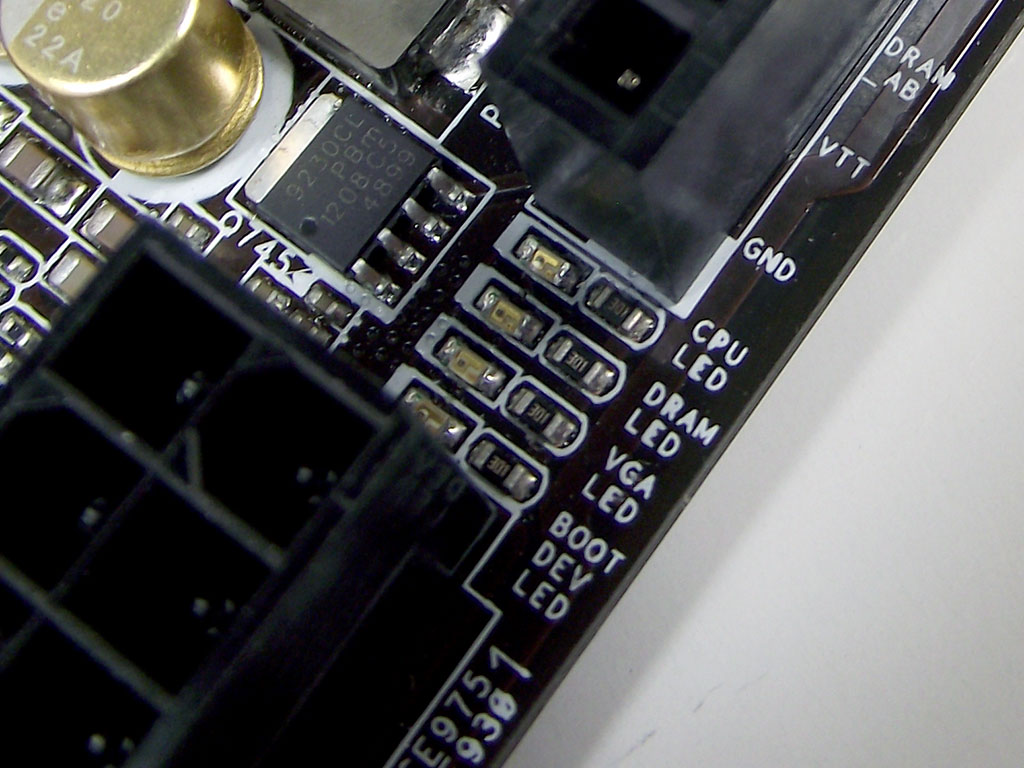
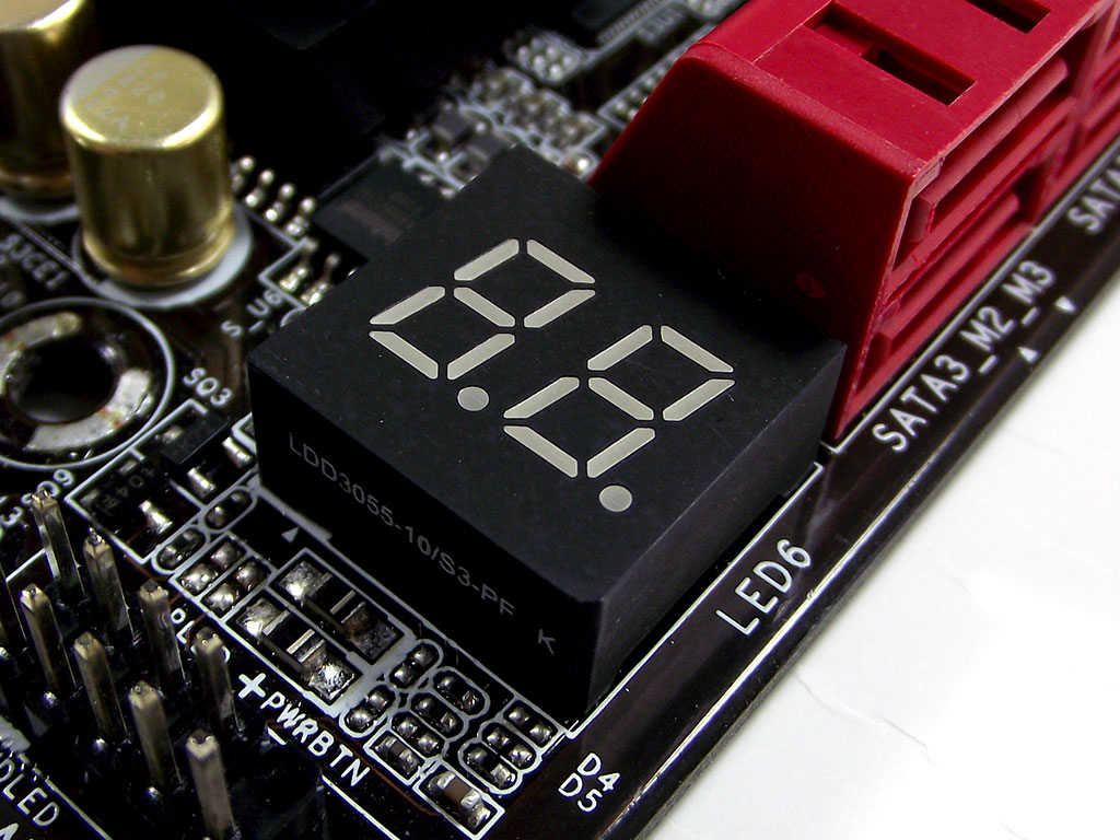
Other pre-OS boot overclocking features include two different POST diagnostic displays and a series of LEDs just above the 24-pin power connector. It's pretty basic, just four LEDs, but it does, at the same time, directly point you to what part of the system may be at fault. Below the SATA ports I found a far more informative dual-digit POST code display which will precisely point to where a boot has failed.
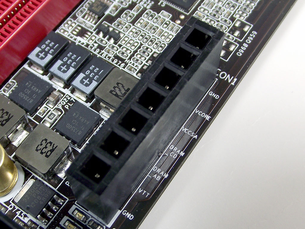
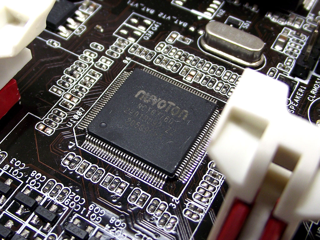
That is not all, as I found a seven-port measurement block meant to be used in conjunction with a digital multimeter, to give accurate real-time voltage monitoring capabilities. Once the board is up and running a Nuvoton NCT6776D Super I/O reports voltage info and provides fan control via software in BIOS or in Windows. It also provides support for the PS/2 keyboard port.
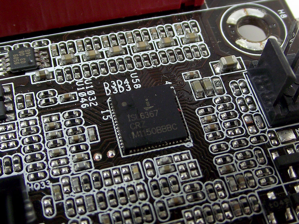
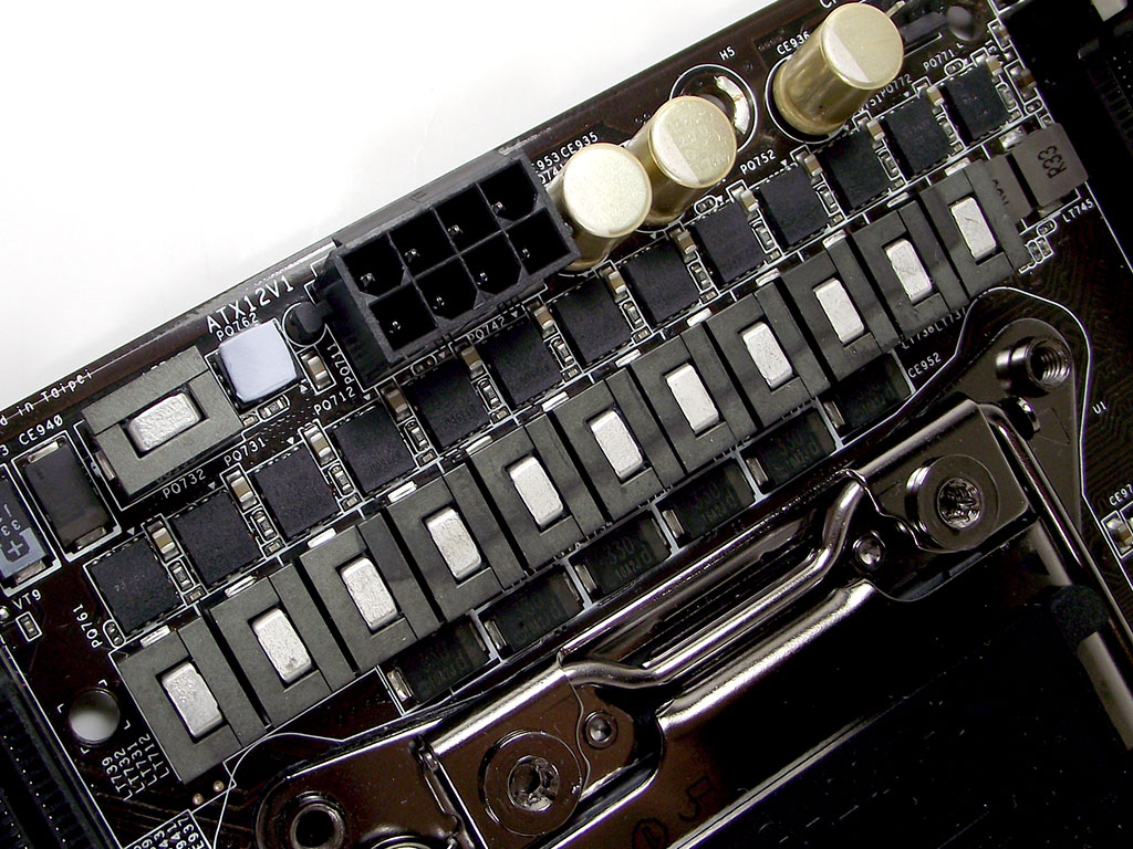
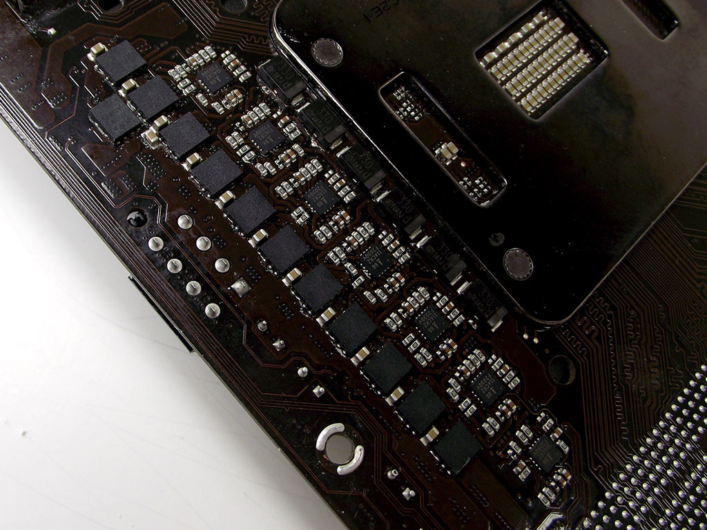
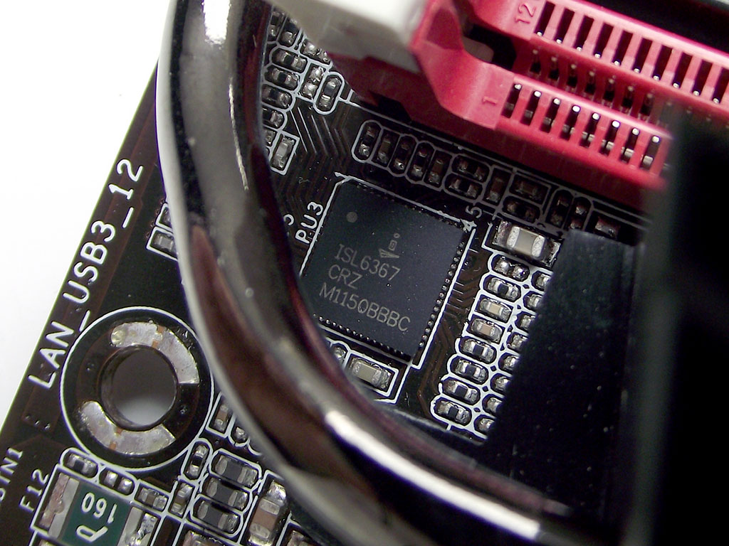
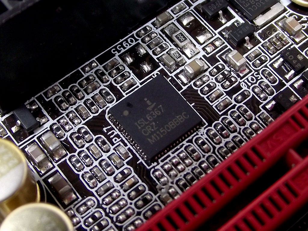
The power delivery for the ASRock Fatal1ty X79 Champion is pretty strong, with an Intersil ISL6367 in control of the CPU VRM. The CPU VRM itself is a 12 + 2 phase design with components found on both the front and the rear of the board just above the CPU socket.
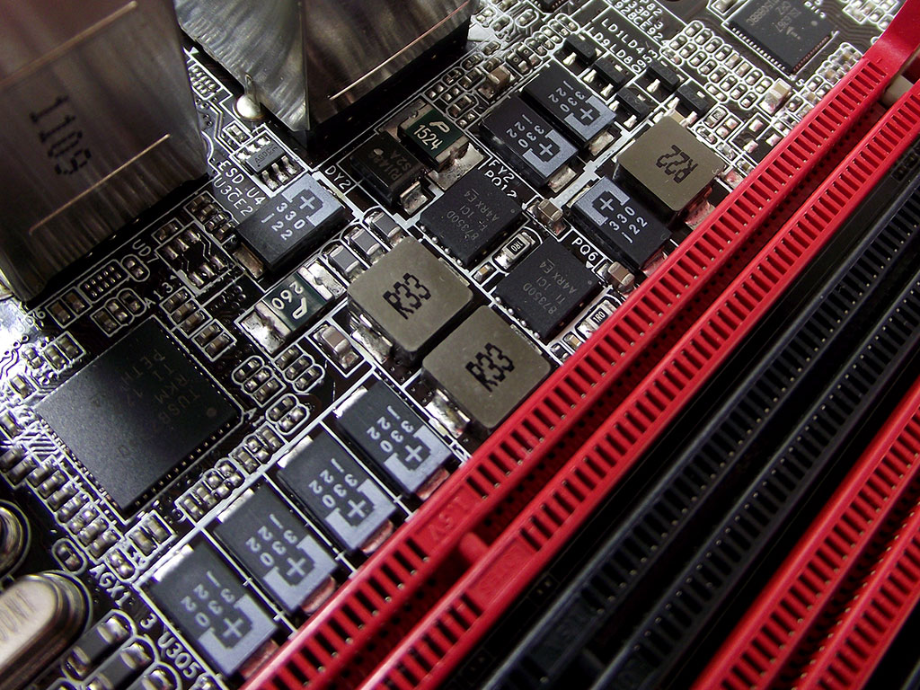
I was surprised to find that there was another Intersil ISL6367 driving at least the DIMM VRM and perhaps more. The left DIMM VRM uses a whole bunch of low-profile surface-mounted components, as part of the cooling solution sits right above the DIMM bank's power delivery section, but the two do not make contact with each other.
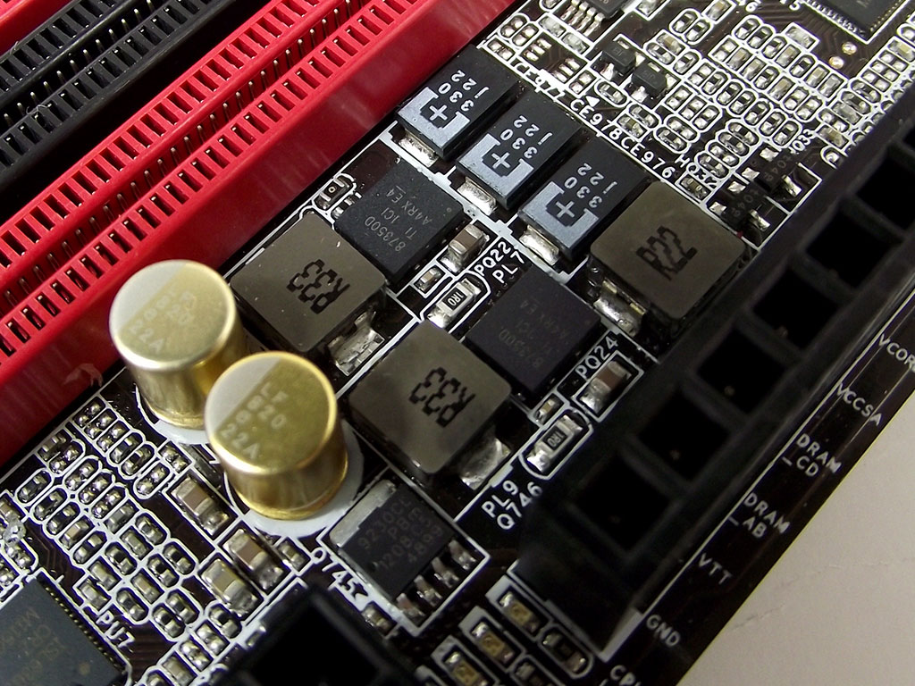
The right DIMM VRM also has its own ISL6367 located between the measuring pin block and the right bank of DIMM slots. The VRM for that bank has a couple of rather normal capacitors although they are gold and stand out a fair bit more in comparison to the opposite bank's VRM design.
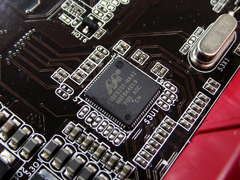
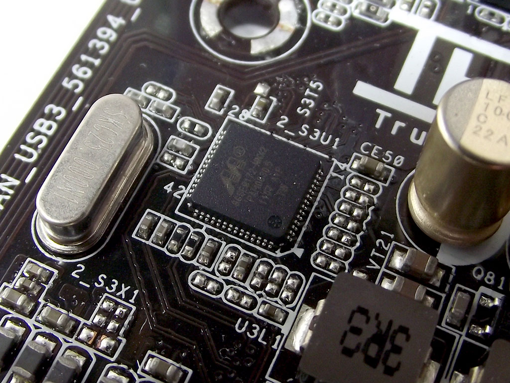
Marvell provides all the SATA control outside of the Intel-provided ports with a 88SE9230 powering all four added internal SATA 6 Gb/s ports. This is a new-for-2012 controller that makes use of a PCIe 2.0 x2 link to ensure adequate bandwidth is provided for all four ports although the link is capped at 1000 MB/s in each direction. I also found a far more common 88SE9172 Marvell controller on the board's left edge which provides the dual eSATA ports on the rear I/O, both of which also support SATA 6 Gb/s speeds.

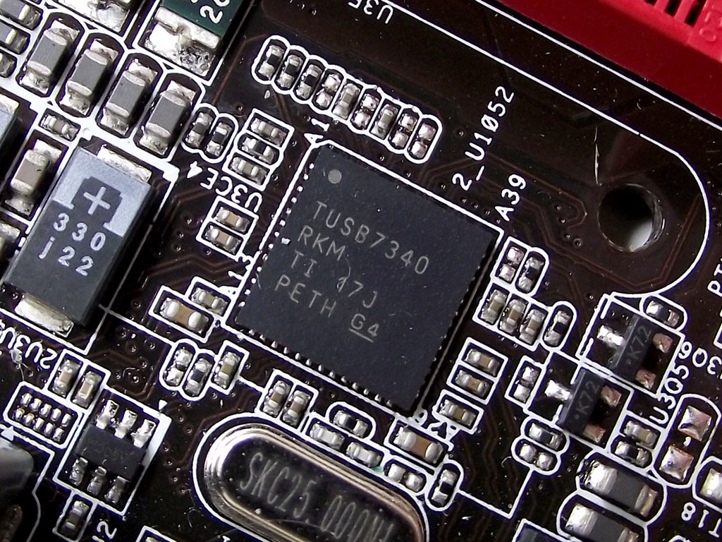
With the huge number of USB 3.0 ports on the ASRock Fatal1ty X79 Champion, I knew I'd find several controllers, all of which are Texas Instruments TUSB7340 controllers.
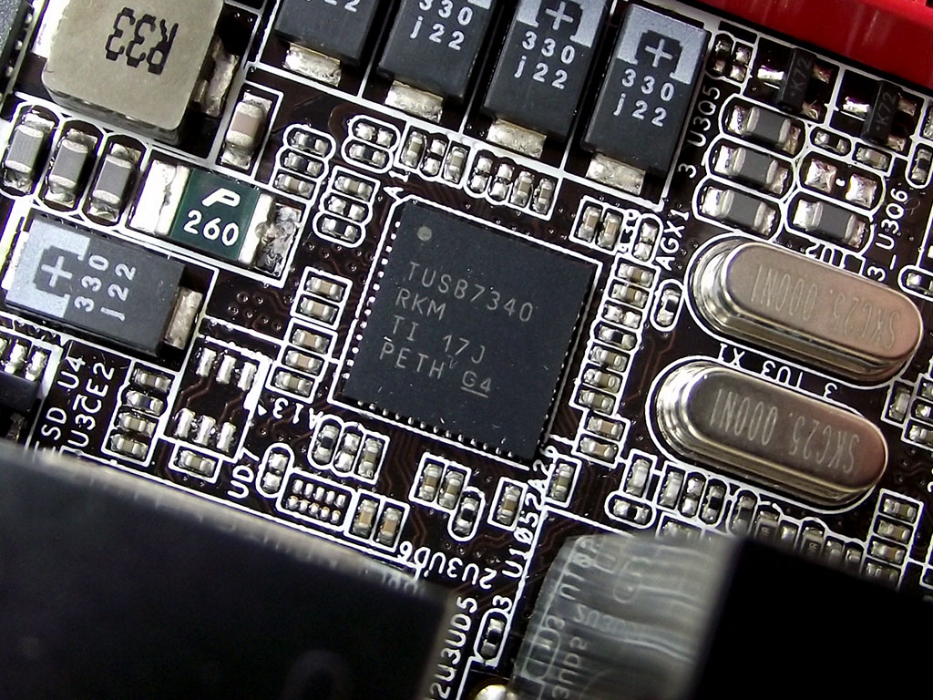
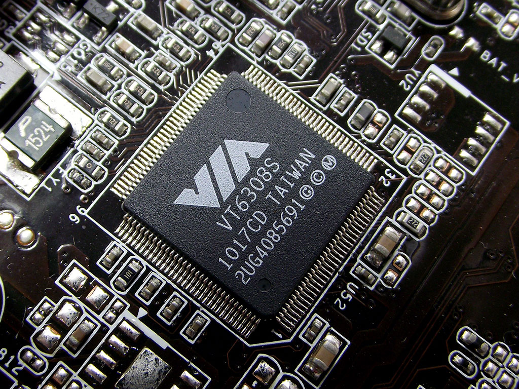
Three controllers total is a whole heck of a lot of USB 3.0 support, seeing how each controller can push four ports total. FireWire is provided by a VIA VT6308S, easily recognized by its bold white lettering.
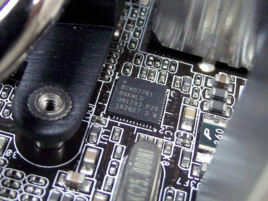
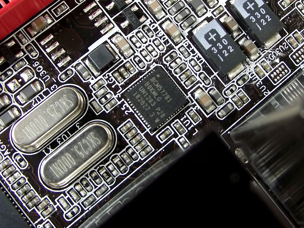
The dual LAN controllers are provided using two Broadcomm BCM57781 chips, both of which are pictured above.
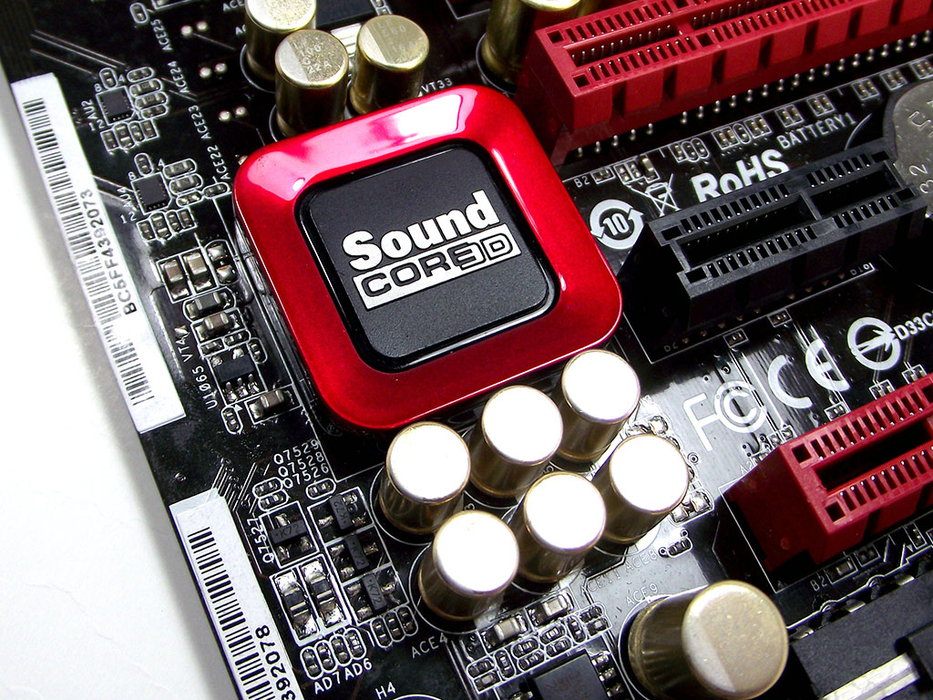
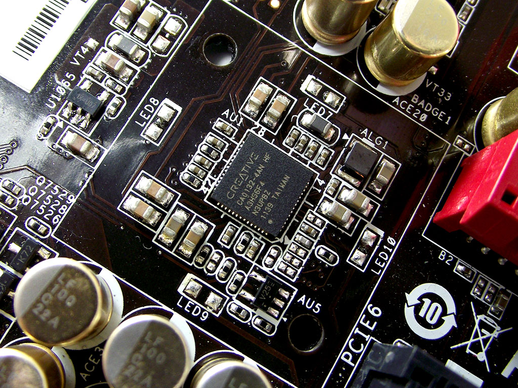
The audio controller is hidden under the red and black plastic cover shown above, which I removed easily as it's just a simple cover secured with a couple of screws on the board's rear side. Underneath I found a Creative CA0132 controller, one that has, recently, exploded on the market and is seen in both discrete products as well as employed by several motherboard OEMs for high-end gaming audio support.
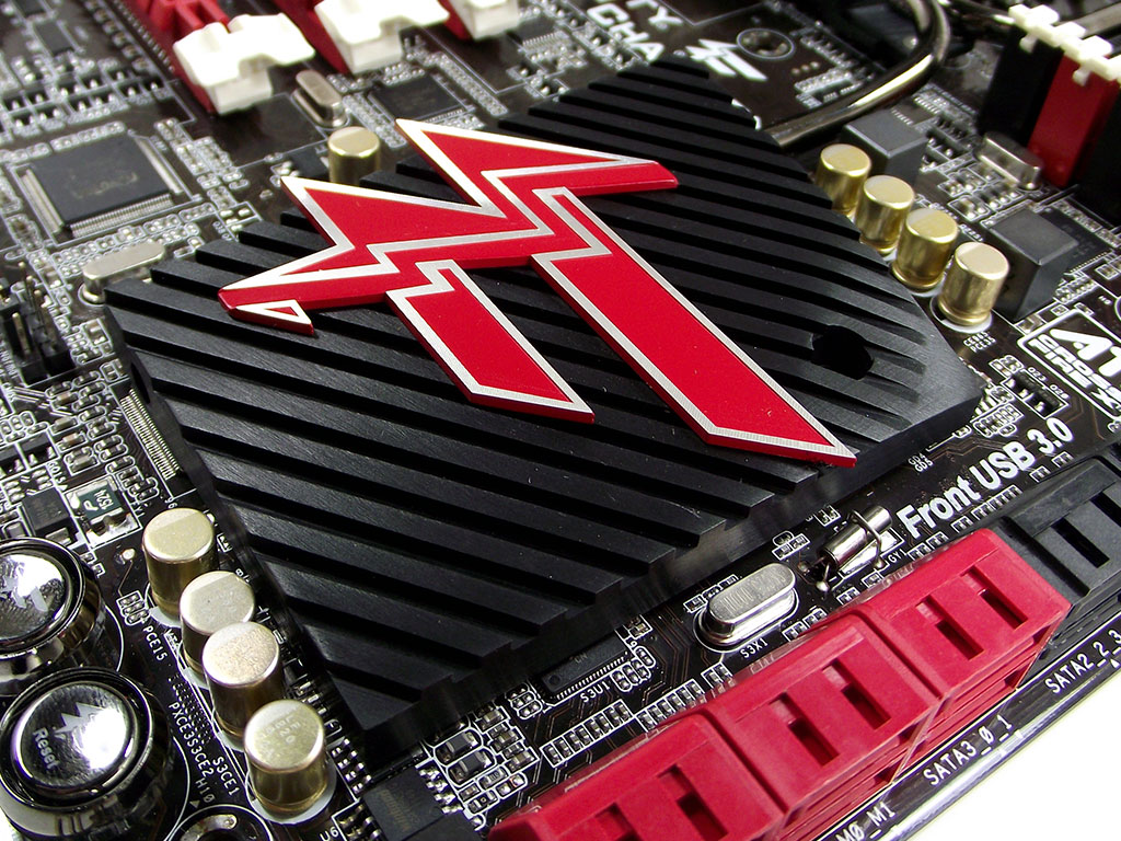
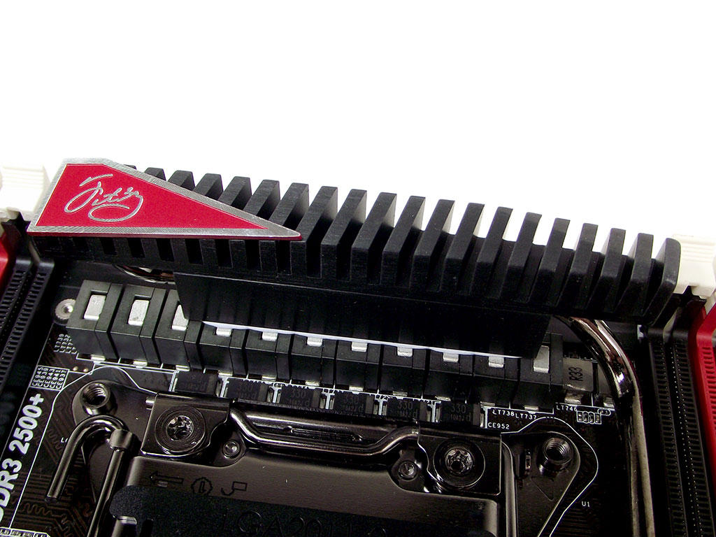
The PCH cooler has a very large Fatal1ty "F" logo in red across a thick-finned black anodized cooling element that attaches to the rest of the board's cooling using a single silver heatpipe. The VRM cooler has Fatal1ty's signature on a vanity plate, affixed to the top of a tall cooler that also contacts the board's chokes, not something I've seen very often.
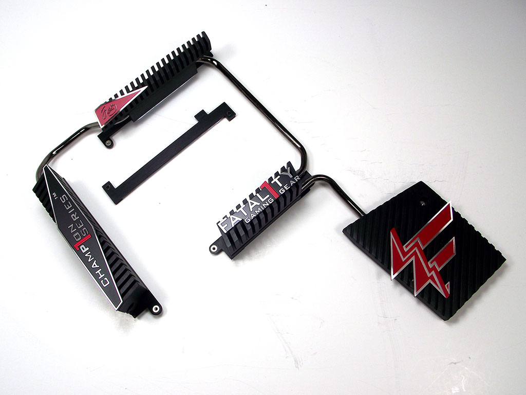
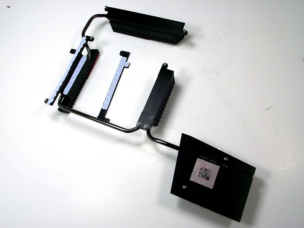
With the cooling removed from the board, the complexity, with the four main elements connected together using heatpipes to transfer heat between them, is pretty obvious. I had to remove nine screws from the cooler before I could begin working at removing the cooler, which did prove a test to the limits of how far I'm willing to go when it comes to board disassembly. Flipping it over I could see excellent contact was made with all critical components, and doing so made it plain that the cooler is really composed of two heat-absorbing parts and two passive radiators that are used to distribute the heat evenly around the board.
Jul 12th, 2025 00:59 CDT
change timezone
Latest GPU Drivers
New Forum Posts
- Can you guess Which game it is? (222)
- 'NVIDIA App' not usable offline? (7)
- What are you playing? (23920)
- RX 9070 XT freezing/locking up only on desktop, anyone else? (43)
- NVIDIA RTX PRO 6000 Workstation Runs Much Hotter Than 5090 FE (22)
- Quick charging your USB devicesUSB 3.2 Gen 2x2 Type-C® front-panel. (1)
- GTX 1050 GPU Owners Club (12)
- ASUS ProArt GeForce RTX 4060 Ti OC Edition 16GB GDDR6 Gaming - nvflash64 VBIOS mismatch (2)
- Will you buy a RTX 5090? (640)
- No offense, here are some things that bother me about your understanding of fans. (33)
Popular Reviews
- Fractal Design Epoch RGB TG Review
- Corsair FRAME 5000D RS Review
- Lexar NM1090 Pro 4 TB Review
- NVIDIA GeForce RTX 5050 8 GB Review
- NZXT N9 X870E Review
- Sapphire Radeon RX 9060 XT Pulse OC 16 GB Review - An Excellent Choice
- AMD Ryzen 7 9800X3D Review - The Best Gaming Processor
- Upcoming Hardware Launches 2025 (Updated May 2025)
- Our Visit to the Hunter Super Computer
- Chieftec Iceberg 360 Review
TPU on YouTube
Controversial News Posts
- Intel's Core Ultra 7 265K and 265KF CPUs Dip Below $250 (288)
- Some Intel Nova Lake CPUs Rumored to Challenge AMD's 3D V-Cache in Desktop Gaming (140)
- AMD Radeon RX 9070 XT Gains 9% Performance at 1440p with Latest Driver, Beats RTX 5070 Ti (131)
- NVIDIA Launches GeForce RTX 5050 for Desktops and Laptops, Starts at $249 (119)
- NVIDIA GeForce RTX 5080 SUPER Could Feature 24 GB Memory, Increased Power Limits (115)
- Microsoft Partners with AMD for Next-gen Xbox Hardware (105)
- Intel "Nova Lake‑S" Series: Seven SKUs, Up to 52 Cores and 150 W TDP (100)
- NVIDIA DLSS Transformer Cuts VRAM Usage by 20% (97)