 48
48
ASRock X79 Extreme11 Intel LGA 2011 Review
BIOS Walkthrough »The Board - A Closer Look

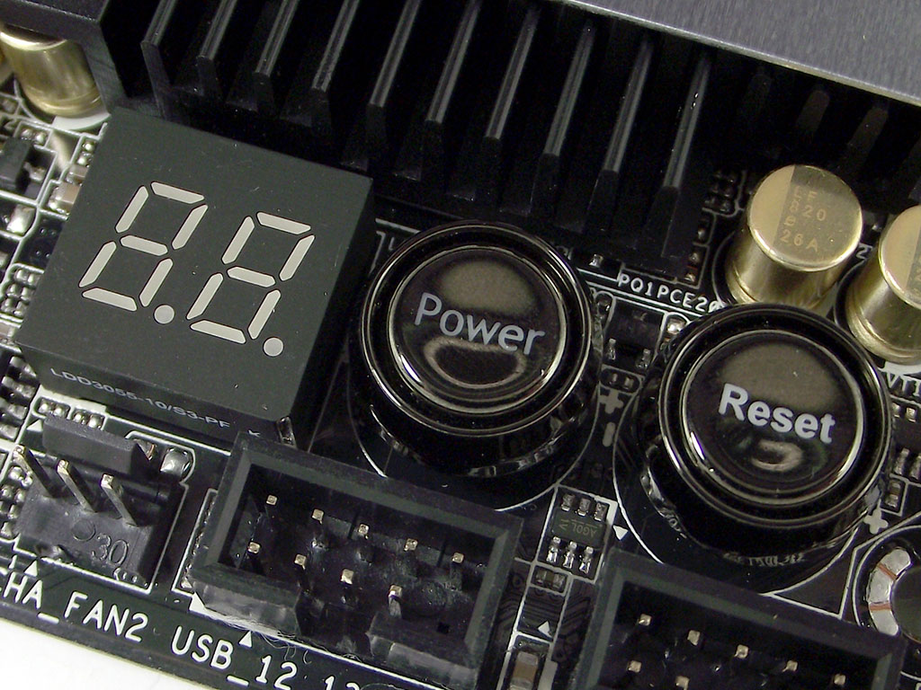
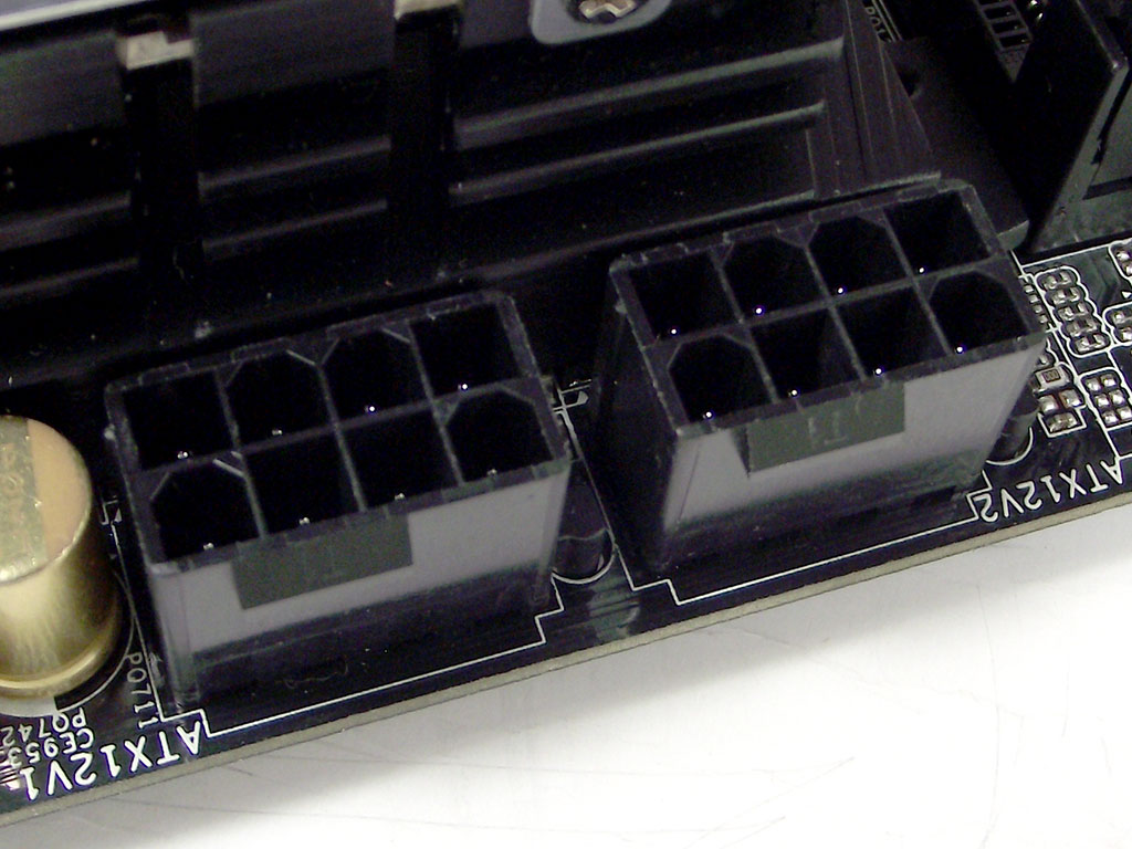
Like many high-end boards today, the ASRock X79 Extreme11 has it's BIOS chip nestled into a socket for easy removal and replacement if need be, or for those who happen to be the sort that likes to swap chips when overclocking. Speaking of overclocking, there are quite a few overclocking features here as well, including a dual-digit POST code display, and Power and Reset switches next to that display on the board's bottom edge. I also noticed that there were not just one, but TWO 8-pin EPS power connectors to provide the CPU with power, while also helping efficiency and temperatures a little bit.
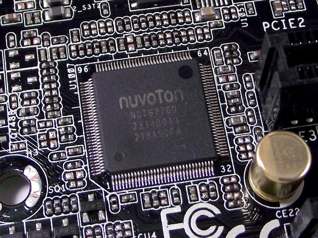
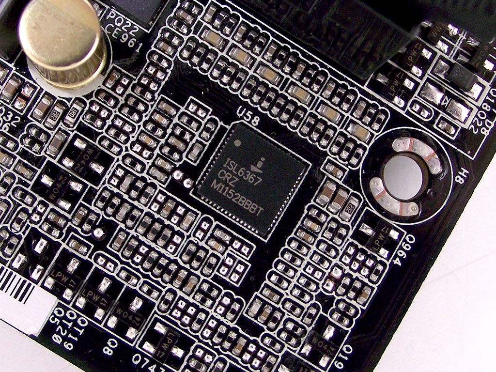
For monitoring duties I located a Nuvoton NCT6776D, a pretty capable Super I/O chip that I've seen before. In charge of VRM control is an ISL6367, yet another commonly used part that has proven itself with time in the retail market.
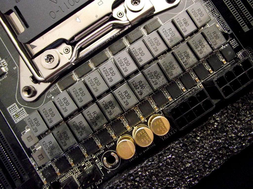
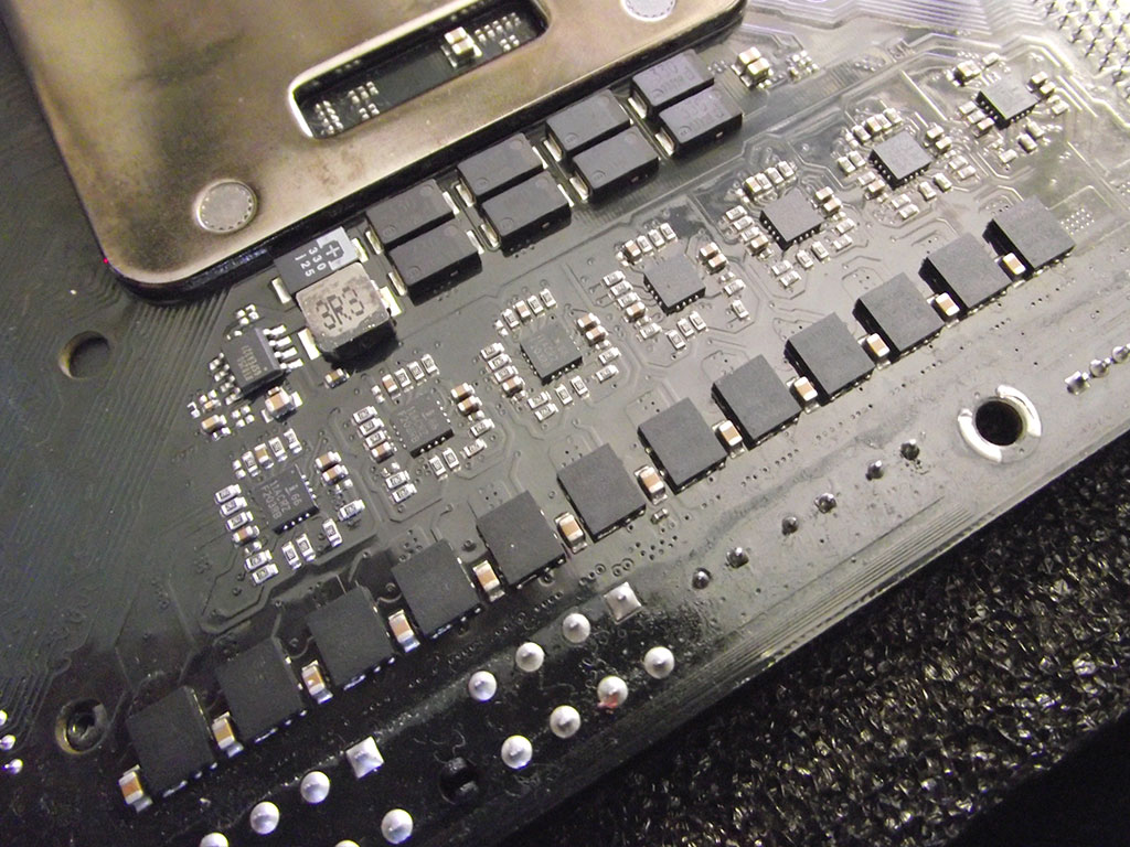
The CPU VRM is pretty crazy I must say! Equipped with 24 phases for the CPU itself, the CPU VRM is so complex that there are a huge number of parts both on the board's top, and the rear. There are two phases for the System Agent as well, and I found seven input drivers on the rear of the board by the socket. This indicates that there would be a minimum of four phases running at any given time, but knowing that the ISL6367 can dynamically adjust the number of phases in use, I'm sure some sort of power-saving technology will be implemented here as well.
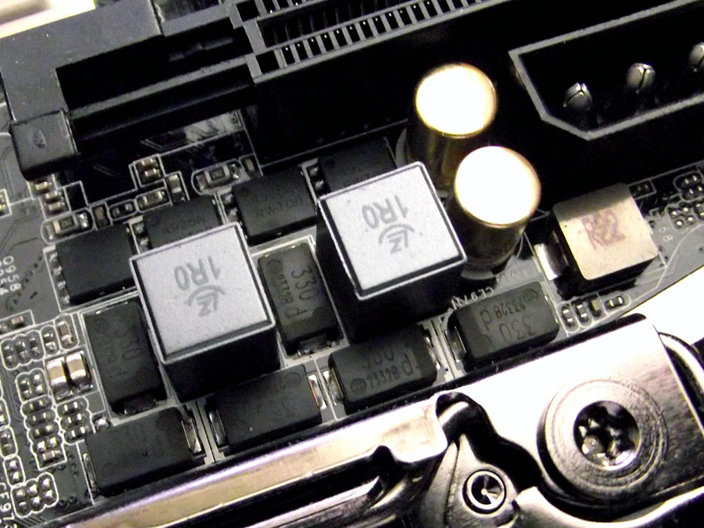
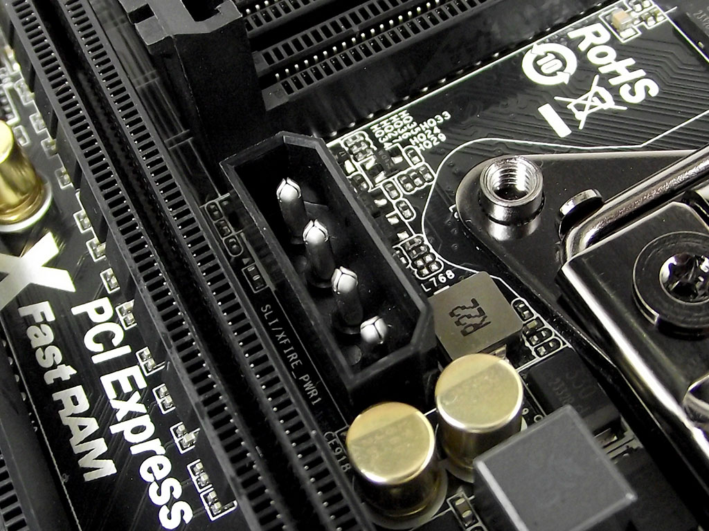
The VTT power phases are located between the socket and the PCIe slots, and also appears to be of a dual-channel design. I found another MOLEX power connector nearby to provide additional power for the PCIe slots, like the MOLEX connector on the board's bottom edge.
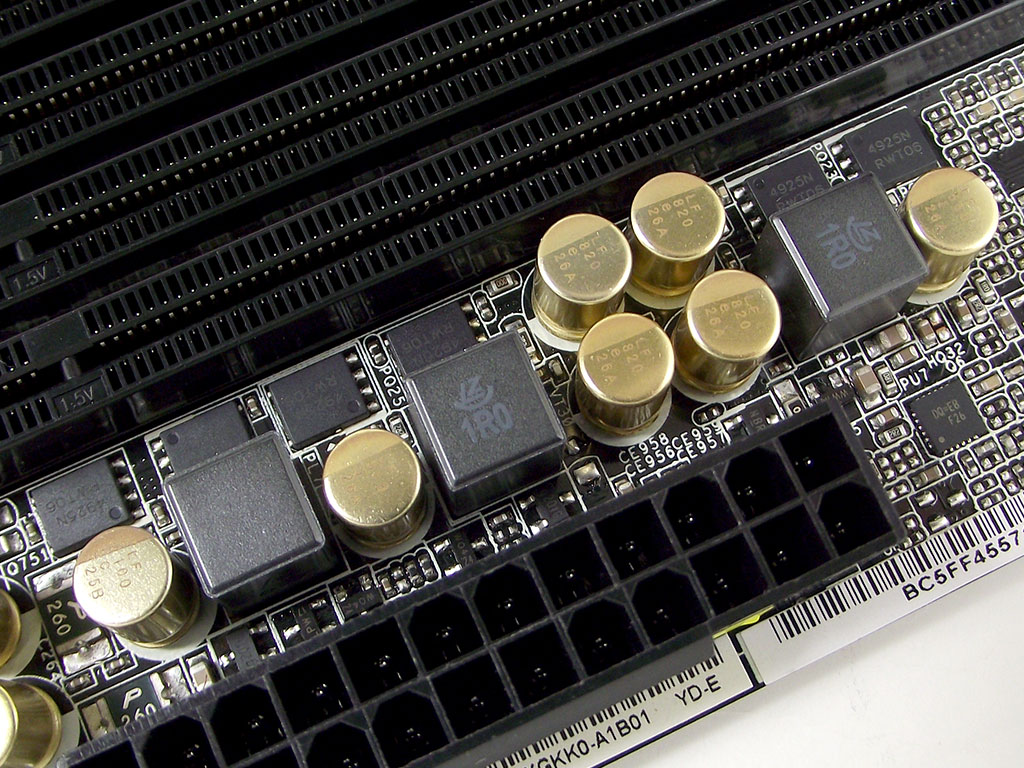
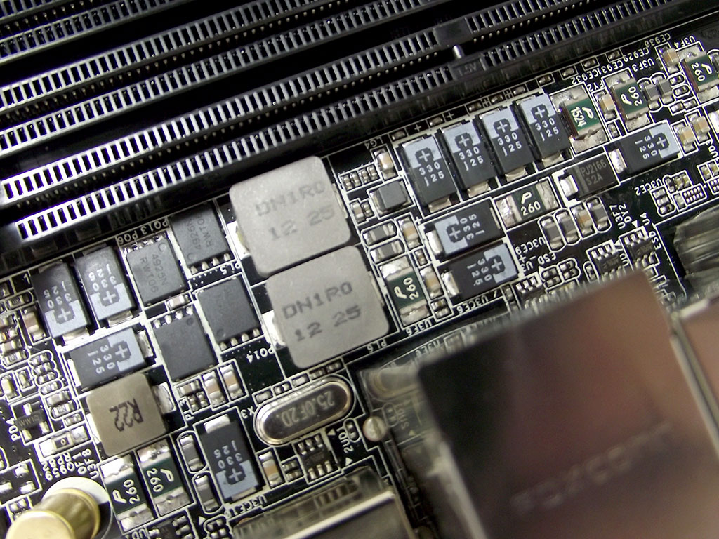
Both DIMM VRMs are dual-channel as well, although they have slightly different component configurations. The power phases for the right bank are right between that bank of slots and the 24-pin power connector, while the VRM for the other bank is between those slots, and the rear I/O area. Both effectively provide the same power, but I personally find it odd ASRock chose two different designs with the left bank using all low-profile parts, and, unlike other boards that use low-profile components for this side, there is no cooler sitting on top of these parts. It's not an issue of quality; parts used on the right bank do tend to be of higher quality than those used on the other side.
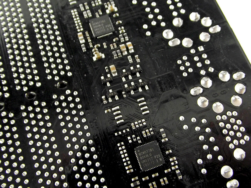
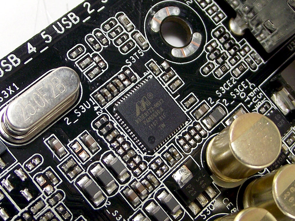
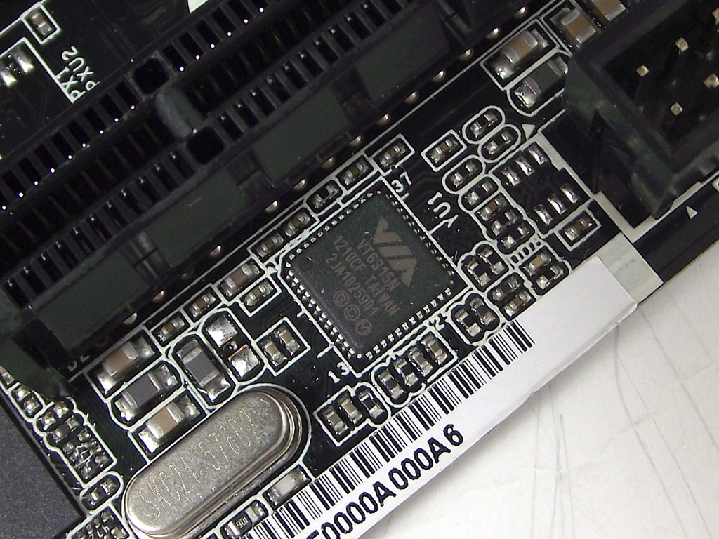
For data I/O duties I found a few different controllers. There are dual Broadcomm BCM57781 LAN controllers, which I found mounted to the back of the board right close to each LAN port. There's a Marvel 88SE9172 SATA 6 Gb/s controller for eSATA control just below the rear I/O blocks, and, lastly, a VIA VT6315N for FireWire support, located on the board's bottom edge.
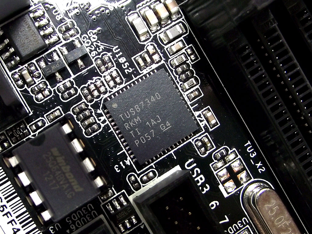
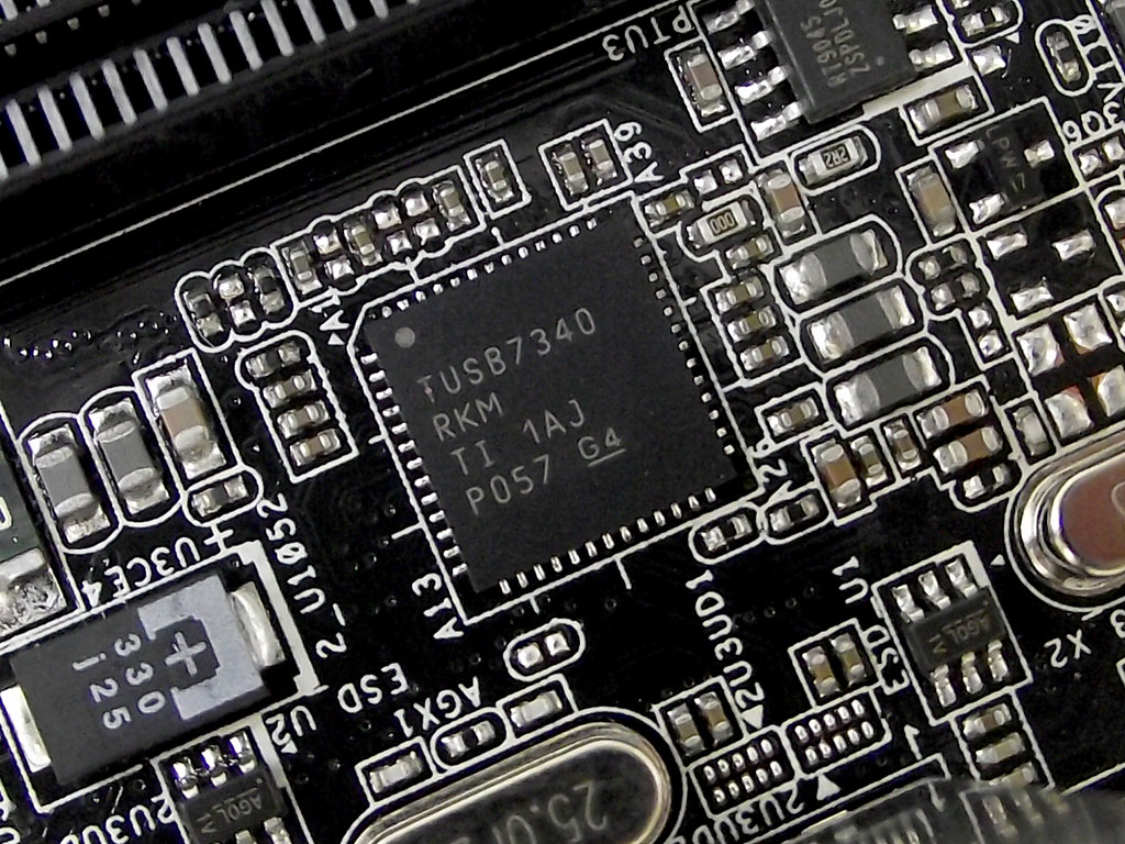
USB 3.0 support is provided by dual Texas Instruments TUSB7340 controller, both of which are capable of pushing four USB 2.0 ports. There's one by the BIOS chip that runs the front I/O USB 3.0, and another located by the PCIe slots, for the USB 3.0 provided on the rear I/O panel.
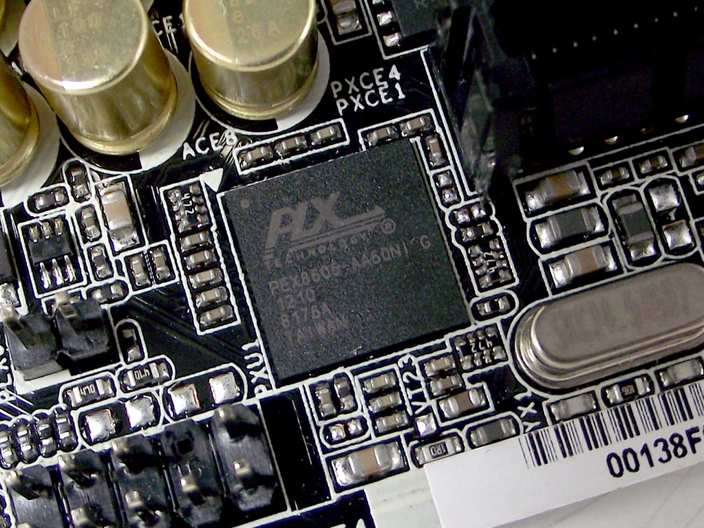
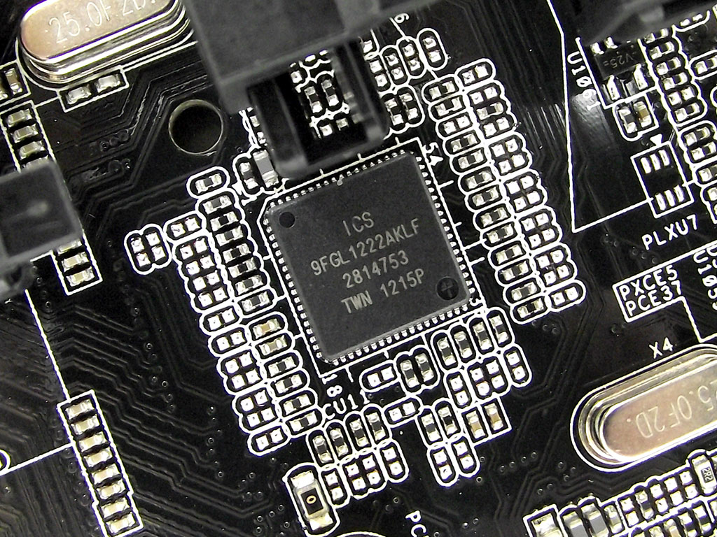
I found a PLX PEX8606 PCIe bridge chip by that VIA FireWire controller, probably there to swap between the FireWire and audio devices. I also located an ICS PCIe Clock Buffer chip, here to stabilize clocks with all those PCIe slots and PCIe devices.
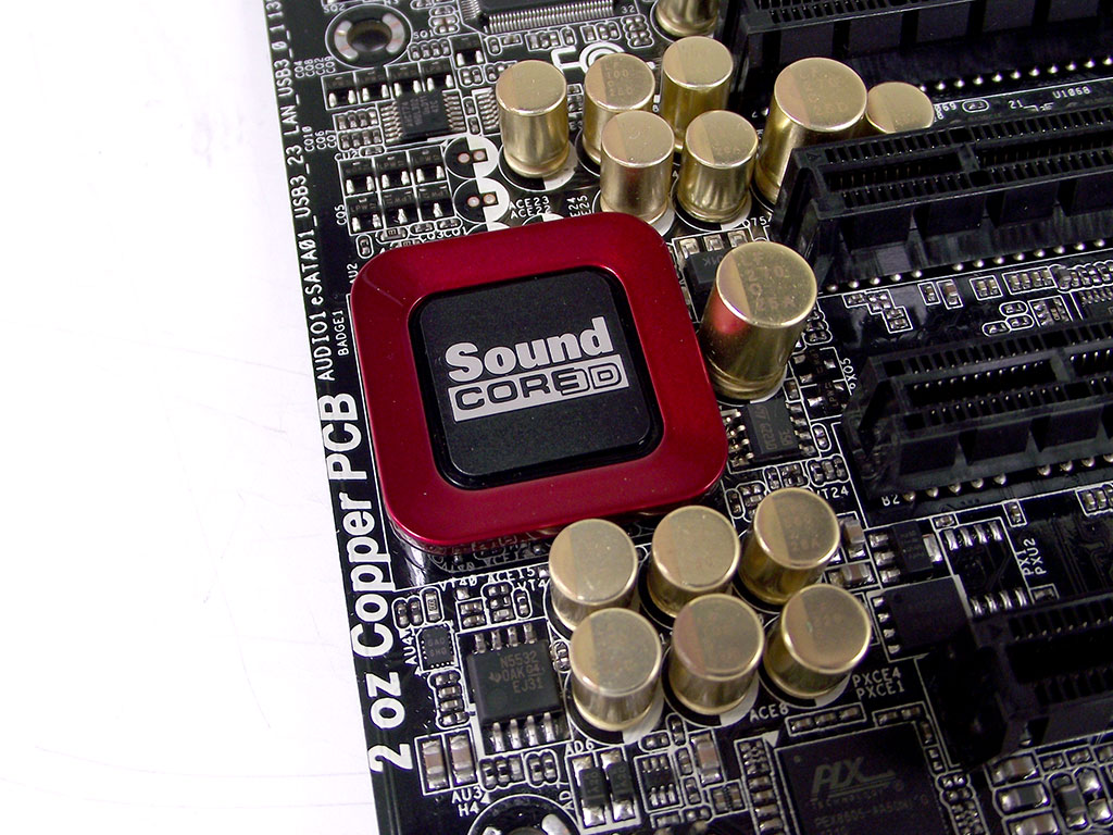
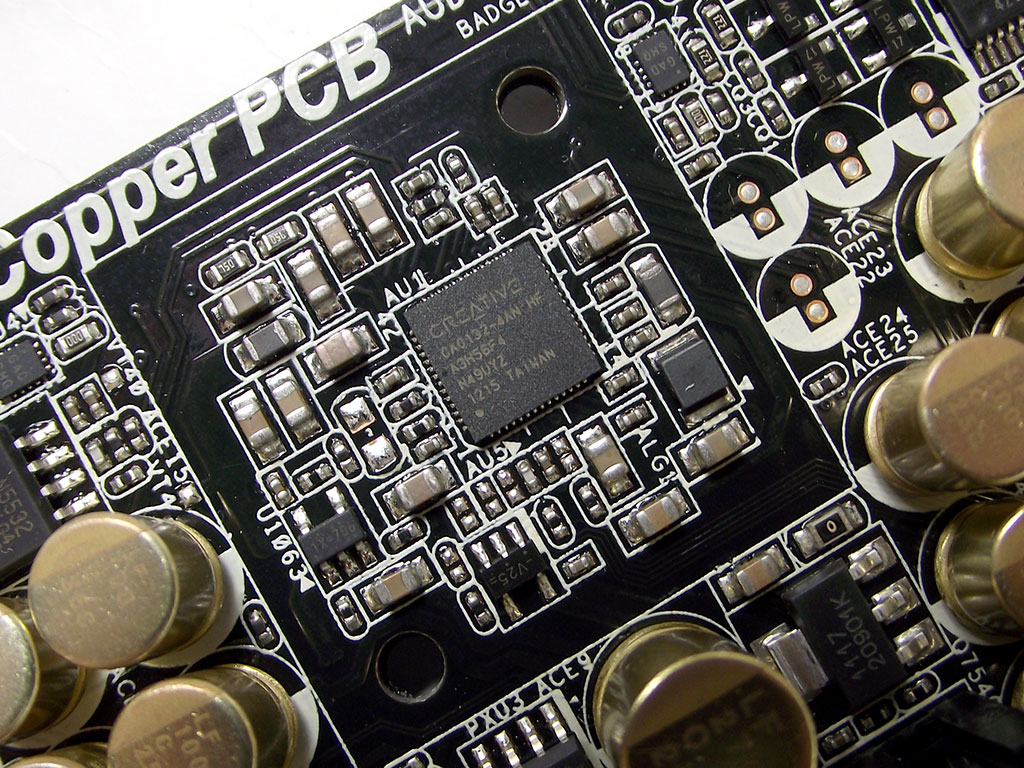
As I mentioned before, the audio is provided by a new Creative Recon3Di chipset, covered with a red plastic top that really stands out. With the cover removed, you can see the actual CODEC itself, a fairly compact chip that has provided some decent audio on more than one motherboard I've tested to date. I am really glad to see it here as well.
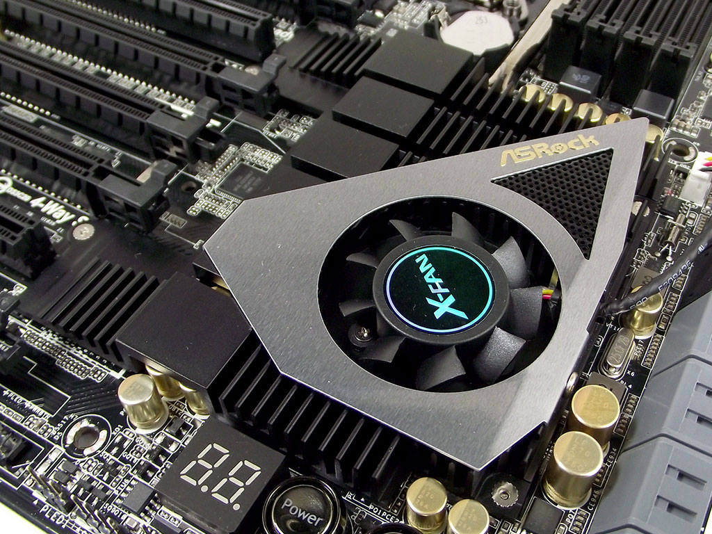
Of course, there's no missing the cooler which is a huge block of metal with a fan sitting just off center. It was pretty easy to remove, and I found quite a few chips underneath of it, which explains why there's a fan here too! I found another ICS clock buffer here as well, situated in the middle of the second pic above.
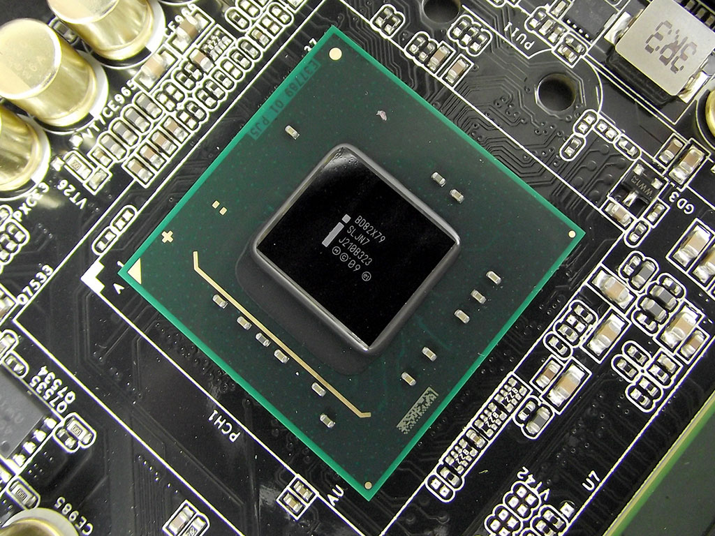
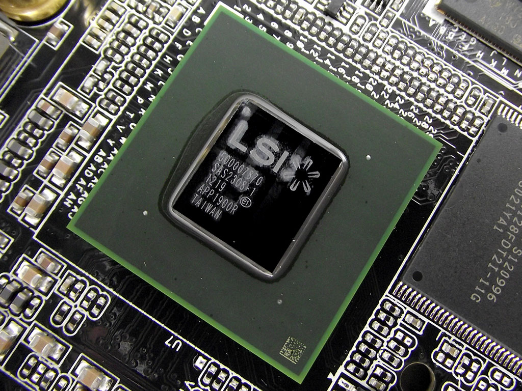
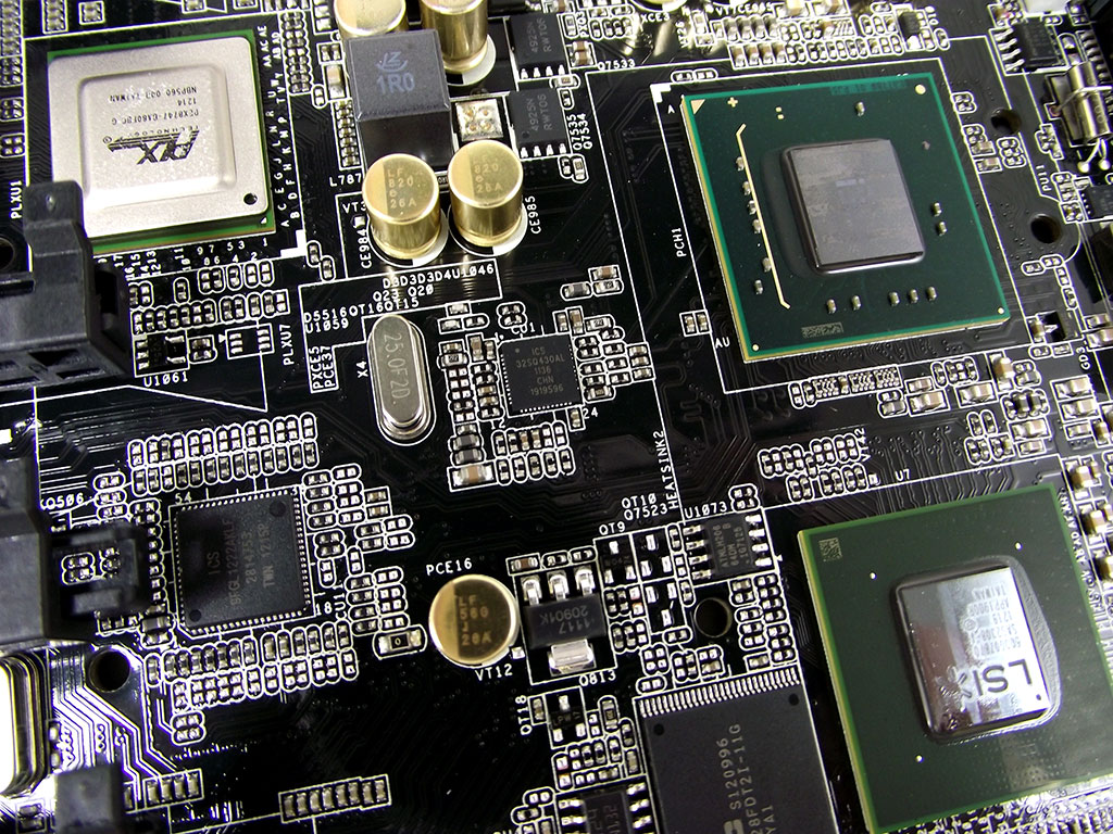
First of all, there's the Intel X79 Express chipset itself, shown in the first image above. Below that is the LSI RAID controller, which was, to say the least, much better than I was expecting. It's a new chip that is PCIe 3.0 compliant, yet it is physically larger than the Intel X79 Express silicon due to using a larger process.
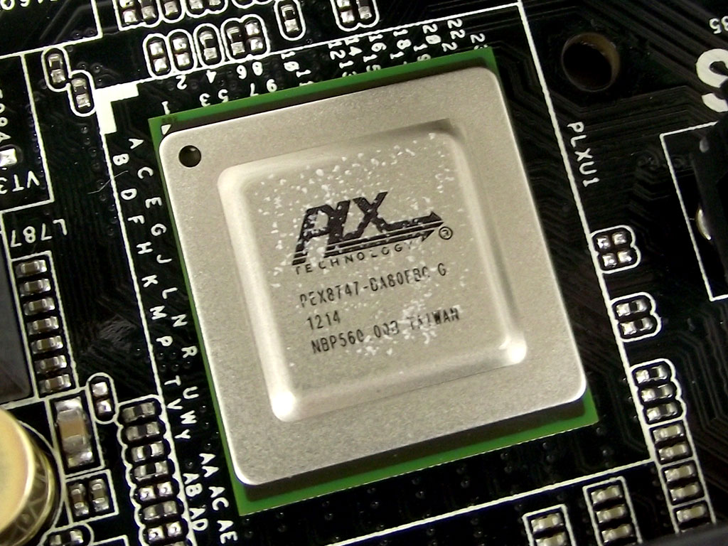
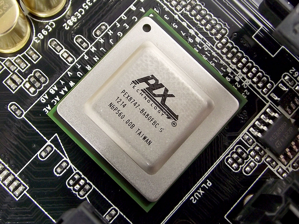
There are also two other large chips below the cooler. I found matching PLX PEX8747 PCIe 3.0 bridge chips capable of pushing 48 lanes each. I think ASRock has simply connected each to one of the PCIe x16 links before doubling that link into dual ports effectively capable of delivering greater bandwidth to PCIe devices than by simply dividing those dual PCIe x16 links from the CPU into four PCIe x8 links. This would leave a direct PCIe x8 link to the CPU for the LSI RAID controller, and provide what I would consider very nearly the best connectivity possible for the X79 platform.
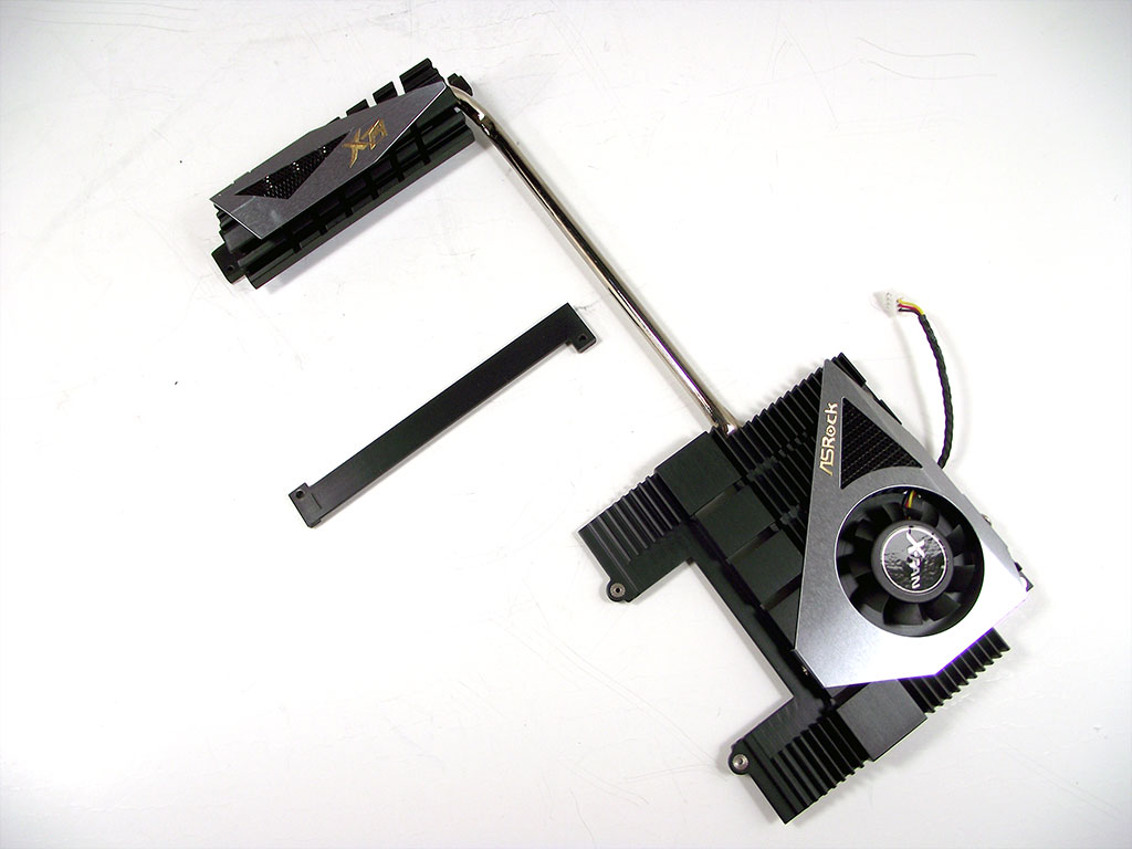
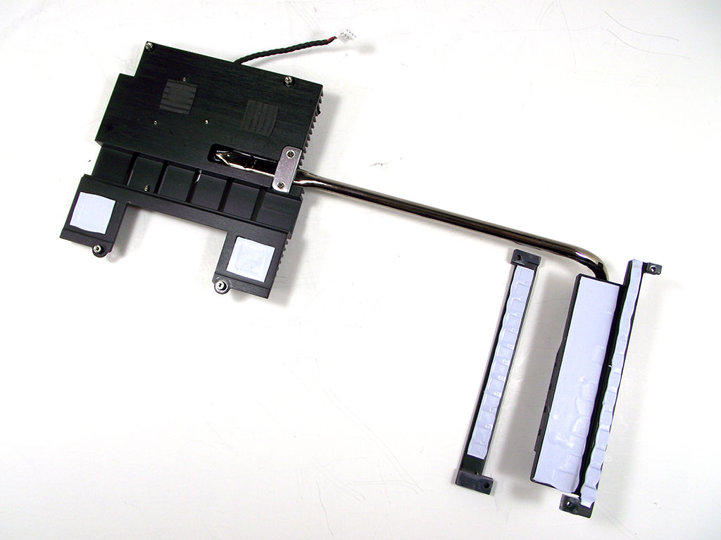
You can see how large the cooler itself really is after I removed it from the board, as well as notice that it's connected to the VRM cooler with a heatpipe, which, after my testing, seems to transfer heat towards the VRM section rather than away from it. Flipping the cooler over, you can see that there are pads here instead of paste due to differing chip heights during assembly, something that is nearly unavoidable with so many different chips all mounting to the same cooler. The heatpipe itself passes over the CPU VRM chokes rather than the MOSFETs, which, with the huge number supplied, shouldn't be running hot at all.
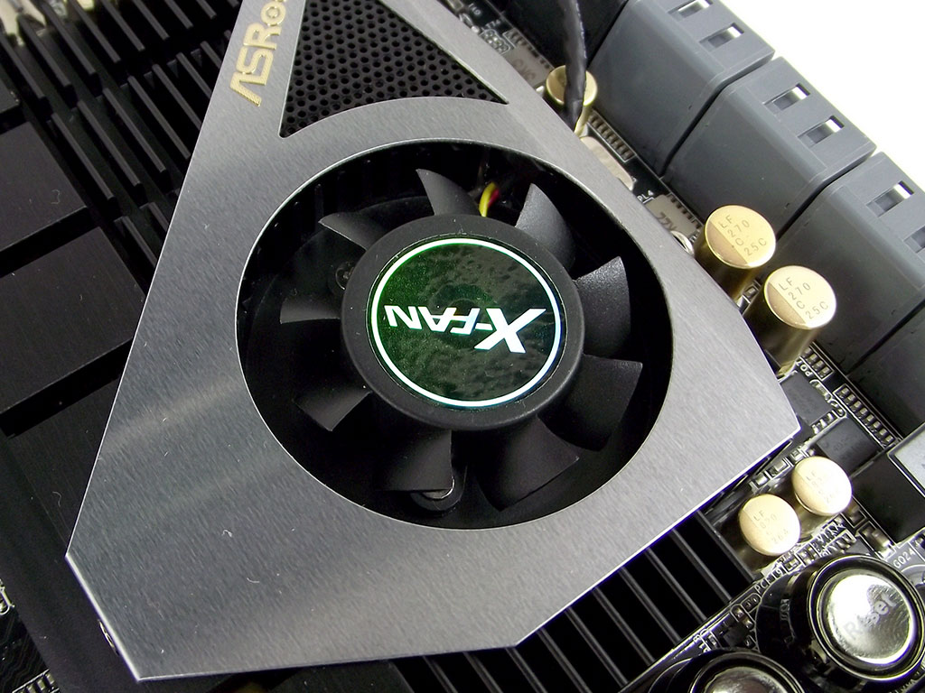
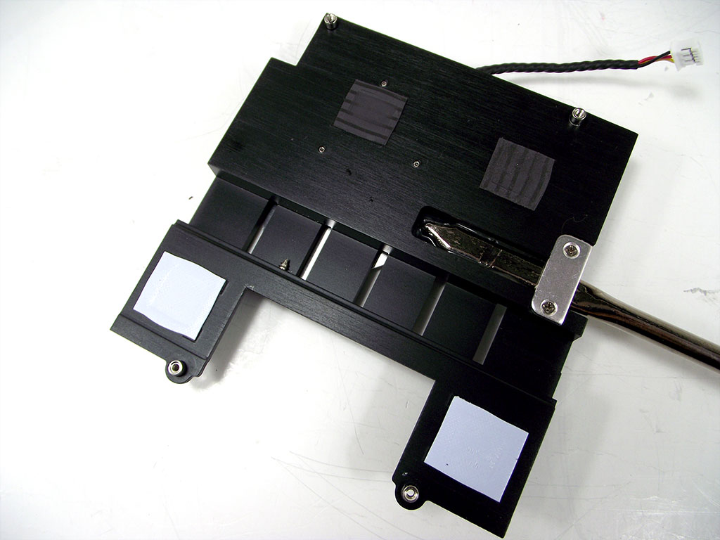
The fan in the cooler is small, perhaps 40mm wide, although it screams like it's 4000 mm in size once the board gets warm. Looking closely at the underside of the cooler, you can see that the heatpipe barely contacts the cooler except for its end, while the bare silicon chips get different pads than the PLX PEX8747 chips do, showing that ASRock put considerable thought into designing this cooler. In use, I found the cooler to be so hot I could barely keep my finger on it. It was probably up to about 40 C or 45 C in actual temps. The sensor that controls the fan in the cooler reported 51 C in BIOS, which seems pretty close to what actual cooler temps should be.
Jul 5th, 2025 13:53 CDT
change timezone
Latest GPU Drivers
New Forum Posts
- AMD RX 9070 XT & RX 9070 non-XT thread (OC, undervolt, benchmarks, ...) (155)
- Are there others on TPU with a dual system (two pc´s in one case)? (12)
- FINAL FANTASY XIV: Dawntrail Official Benchmark (196)
- Help Watercooling my PC (1)
- TPU's Nostalgic Hardware Club (20484)
- How do you view TPU & the internet in general? (With poll) (71)
- GravityMark v1.89 GPU Benchmark (310)
- Optane performance on AMD vs Intel (57)
- EVGA XC GTX 1660 Ti 8GB ROM (8)
- TPU's Rosetta Milestones and Daily Pie Thread (2374)
Popular Reviews
- NVIDIA GeForce RTX 5050 8 GB Review
- Fractal Design Scape Review - Debut Done Right
- Crucial T710 2 TB Review - Record-Breaking Gen 5
- ASUS ROG Crosshair X870E Extreme Review
- PowerColor ALPHYN AM10 Review
- Sapphire Radeon RX 9060 XT Pulse OC 16 GB Review - An Excellent Choice
- Upcoming Hardware Launches 2025 (Updated May 2025)
- AMD Ryzen 7 9800X3D Review - The Best Gaming Processor
- Sapphire Radeon RX 9070 XT Nitro+ Review - Beating NVIDIA
- NVIDIA GeForce RTX 5060 8 GB Review
TPU on YouTube
Controversial News Posts
- Intel's Core Ultra 7 265K and 265KF CPUs Dip Below $250 (288)
- NVIDIA Grabs Market Share, AMD Loses Ground, and Intel Disappears in Latest dGPU Update (212)
- Some Intel Nova Lake CPUs Rumored to Challenge AMD's 3D V-Cache in Desktop Gaming (140)
- NVIDIA GeForce RTX 5080 SUPER Could Feature 24 GB Memory, Increased Power Limits (115)
- NVIDIA Launches GeForce RTX 5050 for Desktops and Laptops, Starts at $249 (105)
- Microsoft Partners with AMD for Next-gen Xbox Hardware (105)
- AMD Radeon RX 9070 XT Gains 9% Performance at 1440p with Latest Driver, Beats RTX 5070 Ti (102)
- Intel "Nova Lake‑S" Series: Seven SKUs, Up to 52 Cores and 150 W TDP (100)