 40
40
ASUS ROG Maximus V Extreme Intel LGA1155 Review
Installation & Performance »The Board - A Closer Look
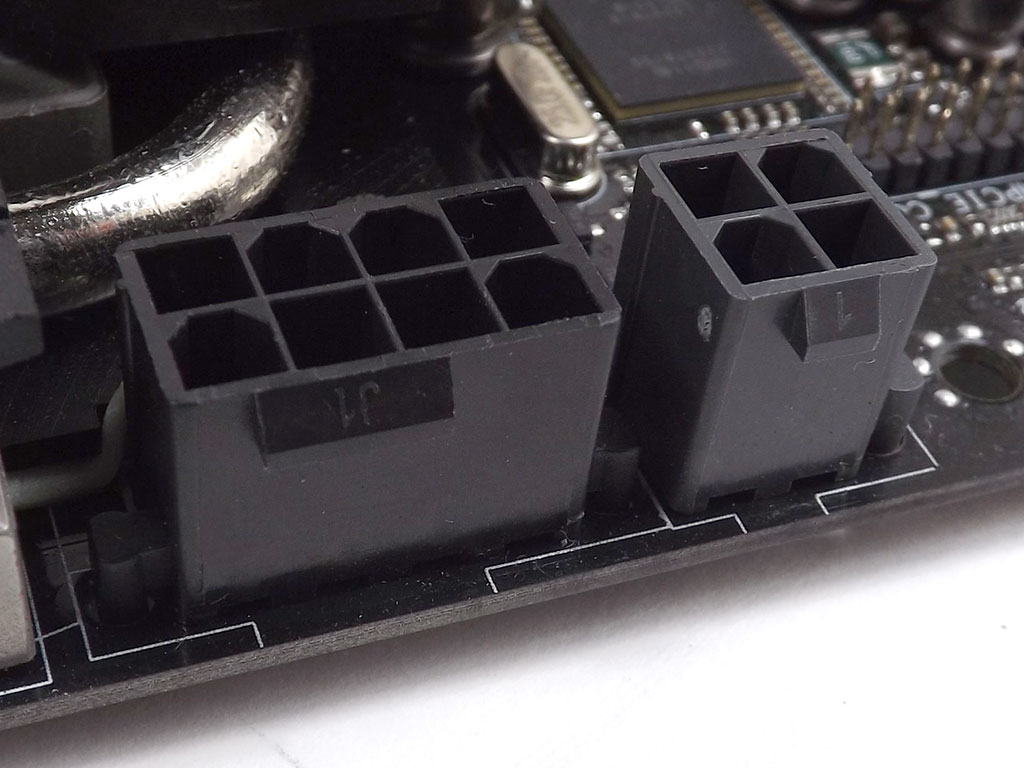
The standard 8-pin EPS connector and an additional 4-pin plug provide power to the board's VRM section. This helps lower the load on each plug and the traces on the board itself, which allows for cleaner power and lower operating temperatures. There are two more plugs to provide the board with power: a white floppy 4-pin plug for adding power to the rear I/O ports and a 6-pin PCIe power plug to add power to the PCIe slots when multiple VGAs are installed.
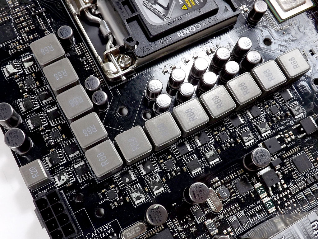
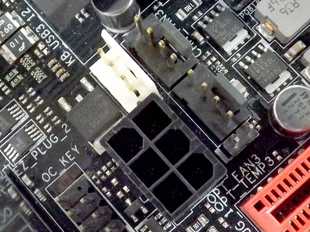
The CPU VRM on the ASUS Maximus V Extreme is managed by a self-branded ASUS DIGI+ part that is shown above. It manages the 8+4 CPU section and provides a wide array of customization options that can found in the BIOS. Each phase is set in pairs, with, as you can see above, a single input driver pushing two phases. The third MOSFET for each of the eight main CPU phases is found on the board's rear, under the black metal backplate. The four iGPU phases don't require as many MOSFETs.

Shown above is the dual-phase DIMM VRM that has its own controller. It manages both phases driven by a singular input drive and offers the same sort of customization as the CPU VRM in the BIOS.
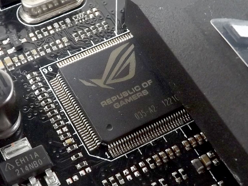
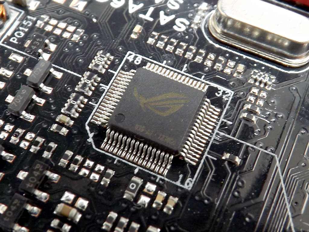
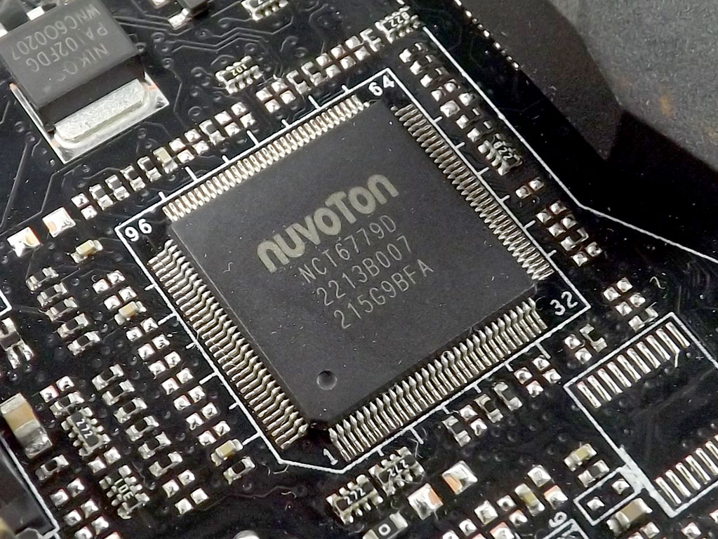
For temperature and voltage monitoring duties and such, I found the usual triplet of dual ASUS ROG-branded chips and a Nuvoton 6779D Super I/O. The smaller chip pictured above has carried the "TPU" label on other boards and offers a similar functionality with the Maximus V Extreme.
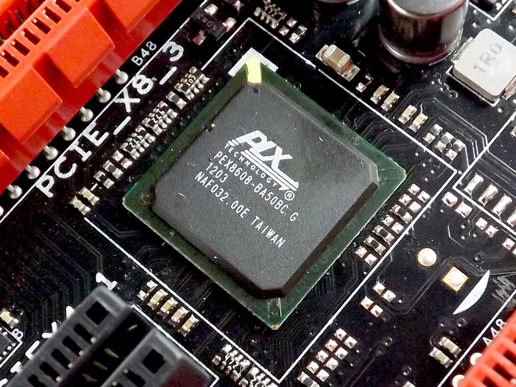

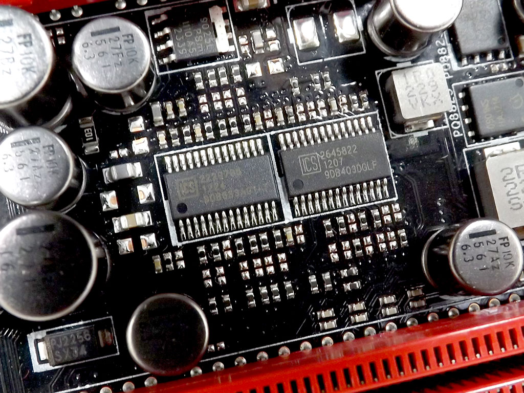
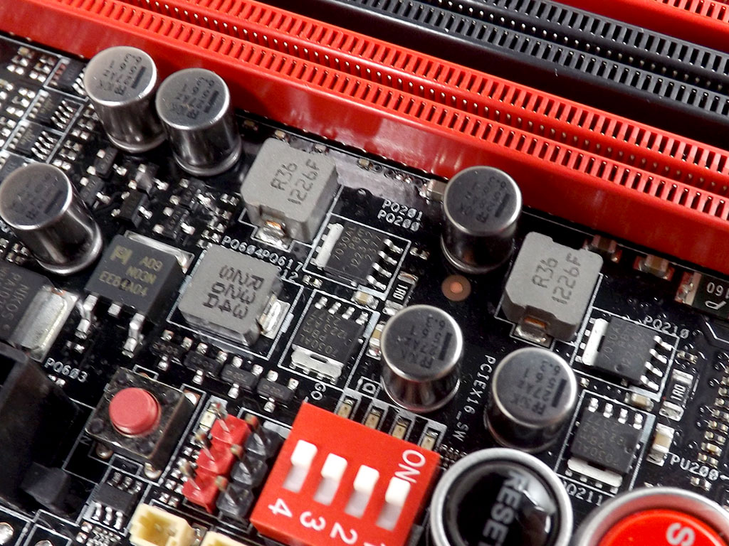
The expansion slots and onboard PCIe devices connect to the system using a pair of PLX PCIe bridge chips. A PLX PEX8608 manages the onboard devices, while the ever-popular PLX PEX8747 PCIE 3.0 bridge chip manages PCIe slot connectivity by splitting the singular PCIe link of your installed GPU off to the four red PCIe x16 slots, each with its own PCIe x8 electrical connection. The difference to other boards is that there is always a direct link to the CPU via the uppermost PCIe slot. The secondary x8 link that comes from the CPU services the PLX PEX8747 chip, which means that three cards are - with four installed cards - sharing a single PCIe x8 link to the CPU. So much complexity to the PCIe sub-complex means that all those ports need some help in bolstering signal integrity if you want to adjust the BCLK, and I found dual ICS clockgen chips for just that purpose. ASUS really has gone the extra mile with the Maximus V Extreme.
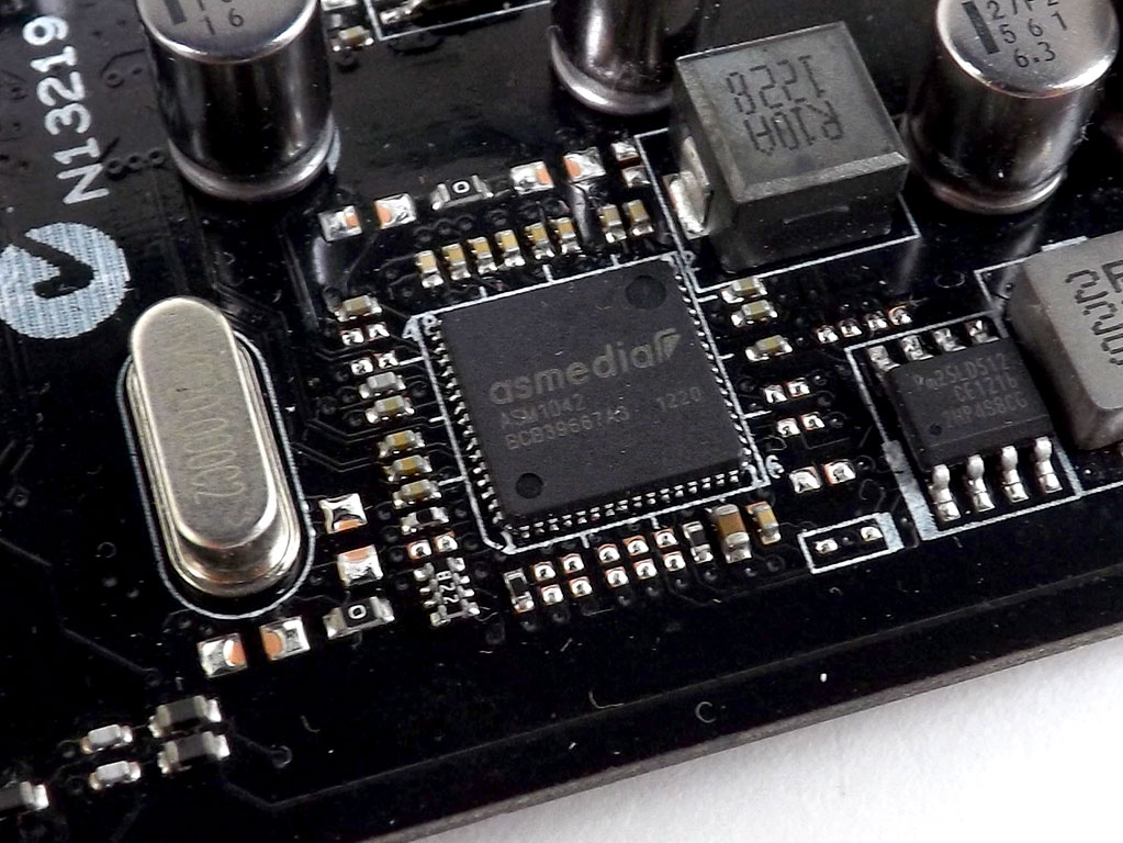
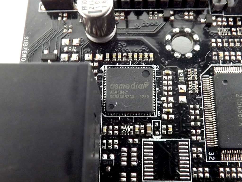
To add in the extra SATA connectivity, there are two ASMedia ASM1042 SATA 6 Gb/s controllers - one above and one beside the internal SATA ports.
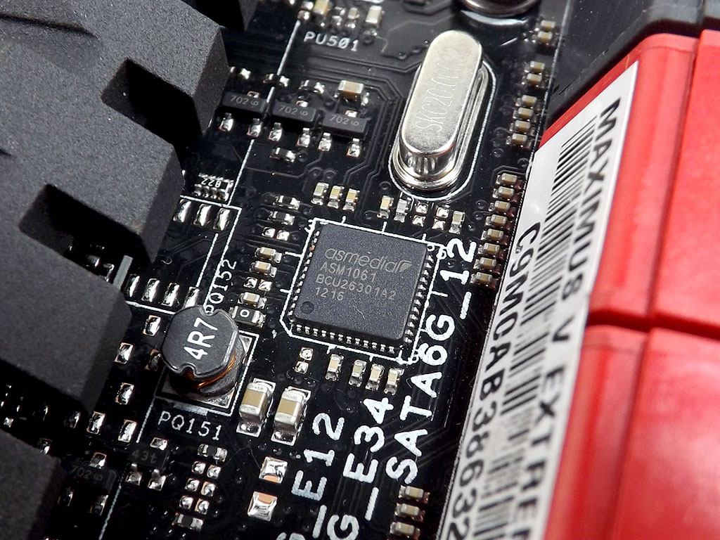

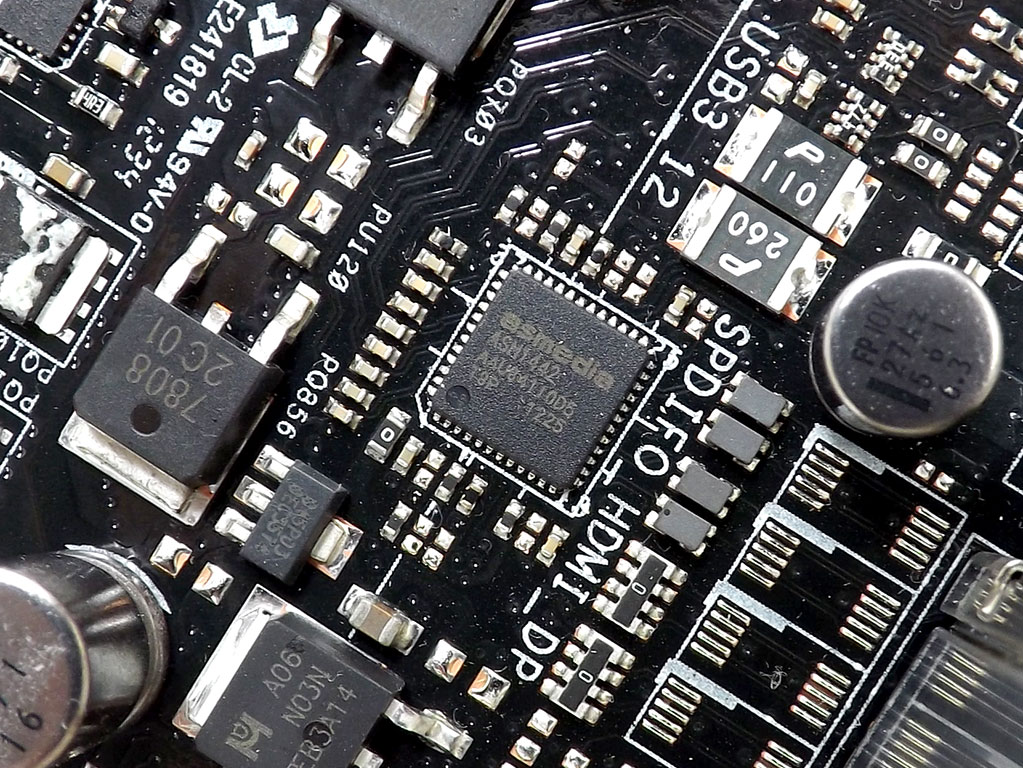
ASMedia also provides the external USB 3.0 controllers and the ASM1442 TMDS switch for HDMI shifting.
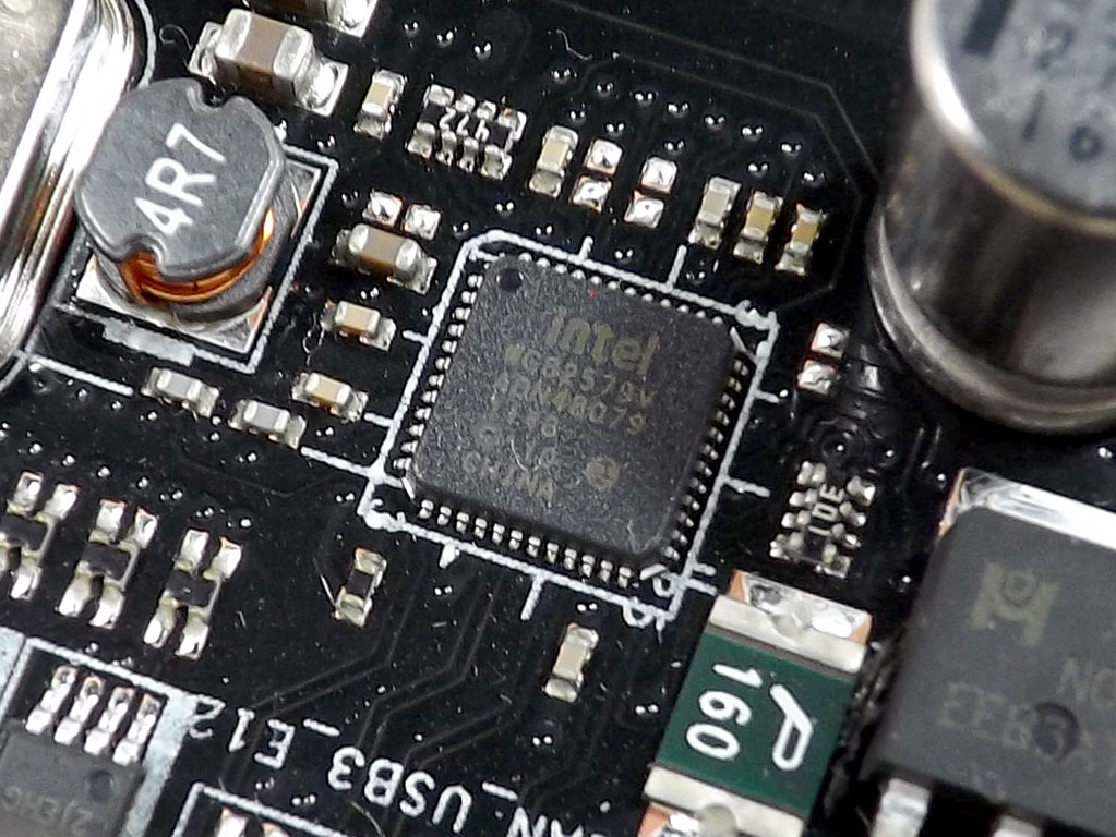
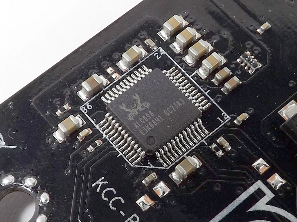
There is an Intel LAN controller, a favorite of many enthusiasts out there, and a Realtek ALC898 audio controller for high-quality audio.
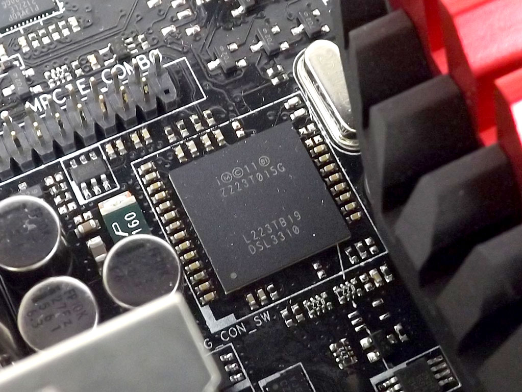
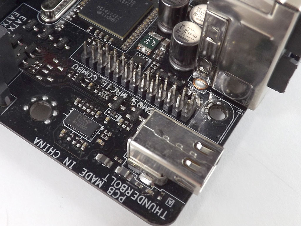
The ThunderBolt controller is near the port itself. The pin header for the WI-FI GO! card is also there.
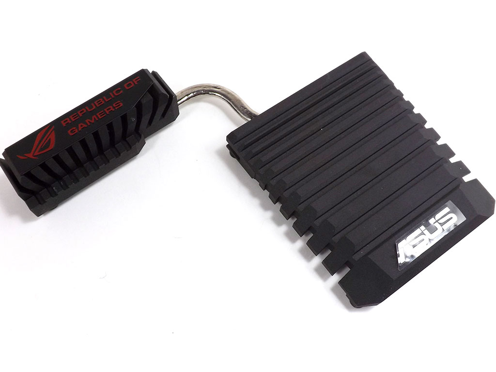
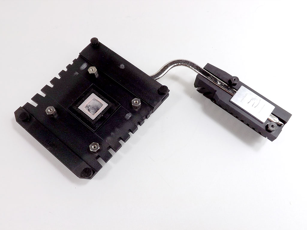
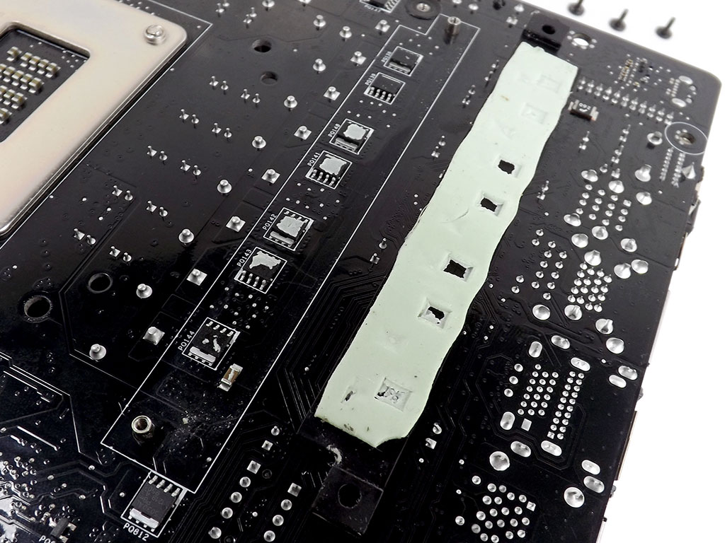
The cooling solution on the ASUS Maximus V Extreme is thick and heavy. Once removed, it's pretty obvious that this is one serious cooler. The lower cooler makes excellent contact with both the PLLX PEX8747 and the Intel Z77 Express PCH. I don't suggest removing them unless you plan to watercool the board. No need to re-paste coolers on this board!
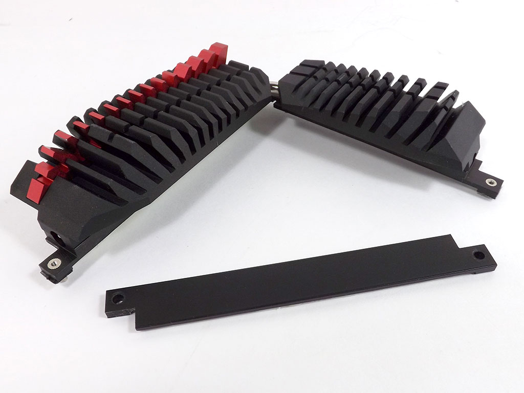
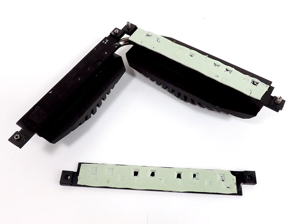
The VRM cooler makes great contact as well. Both sets of coolers are joined by a single heatpipe, and each passive radiator with red accents is made of one large chunk of metal. They became warm to the touch under load testing, but not overly so thanks to their large mass.
Jul 12th, 2025 01:20 CDT
change timezone
Latest GPU Drivers
New Forum Posts
- Will you buy a RTX 5090? (642)
- 'NVIDIA App' not usable offline? (8)
- Can you guess Which game it is? (222)
- What are you playing? (23920)
- RX 9070 XT freezing/locking up only on desktop, anyone else? (43)
- NVIDIA RTX PRO 6000 Workstation Runs Much Hotter Than 5090 FE (22)
- Quick charging your USB devicesUSB 3.2 Gen 2x2 Type-C® front-panel. (1)
- GTX 1050 GPU Owners Club (12)
- ASUS ProArt GeForce RTX 4060 Ti OC Edition 16GB GDDR6 Gaming - nvflash64 VBIOS mismatch (2)
- No offense, here are some things that bother me about your understanding of fans. (33)
Popular Reviews
- Fractal Design Epoch RGB TG Review
- Corsair FRAME 5000D RS Review
- Lexar NM1090 Pro 4 TB Review
- NVIDIA GeForce RTX 5050 8 GB Review
- NZXT N9 X870E Review
- Sapphire Radeon RX 9060 XT Pulse OC 16 GB Review - An Excellent Choice
- AMD Ryzen 7 9800X3D Review - The Best Gaming Processor
- Upcoming Hardware Launches 2025 (Updated May 2025)
- Our Visit to the Hunter Super Computer
- Chieftec Iceberg 360 Review
TPU on YouTube
Controversial News Posts
- Intel's Core Ultra 7 265K and 265KF CPUs Dip Below $250 (288)
- Some Intel Nova Lake CPUs Rumored to Challenge AMD's 3D V-Cache in Desktop Gaming (140)
- AMD Radeon RX 9070 XT Gains 9% Performance at 1440p with Latest Driver, Beats RTX 5070 Ti (131)
- NVIDIA Launches GeForce RTX 5050 for Desktops and Laptops, Starts at $249 (119)
- NVIDIA GeForce RTX 5080 SUPER Could Feature 24 GB Memory, Increased Power Limits (115)
- Microsoft Partners with AMD for Next-gen Xbox Hardware (105)
- Intel "Nova Lake‑S" Series: Seven SKUs, Up to 52 Cores and 150 W TDP (100)
- NVIDIA DLSS Transformer Cuts VRAM Usage by 20% (97)