 24
24
HIS Radeon HD 6950 2 GB Review
Packaging & Contents »Architecture

Cayman, named after the lovely Cayman islands in the Caribbean, is AMD's new high-end GPU. It succeeds Cypress, on which were based Radeon HD 5800 series and the dual-GPU HD 5970. Cayman is built on existing 40 nm process at TSMC. Apart from the processor most of the components inside are the same as the ones found in the previous generation GPUs, except that the hierarchy of components is changed to add a degree of parallelism that goes a step ahead of even Barts. The SIMD cores are completely restructured, too.
With Cypress, there was only one graphics engine (that which computes preliminary data and instructions, and passes them on for low-level processing to the SIMD cores), and one dispatch processor that funneled data and instructions down to the two SIMD engine blocks. Barts introduced a degree of parallelism by giving each SIMD engine block its own dispatch processor, instruction and constant caches. Cayman is taking that a step further, by splitting even the graphics engines between the two SIMD engine blocks. This gives dedicated rasterizers, geometry assemblers to each block, but more importantly, doubles the number of tessellation units, with each graphics engine having one.
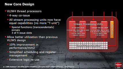
As mentioned earlier, AMD brought about a radical change in the stream processor design. Compared to the older VLIW5 design in which an SIMD core consisted of four simple and one complex stream processors with some common resources, the new design, dubbed VLIW4, combines four equally-capable complex stream processors, with two of the four getting special functions. Overall, with a stream processor count of 1536, the Radeon HD 6970 clocked at 880 MHz, is able to churn out a single-precision floating point (IEEE754-SP) performance of 2.7 TFLOPs, and double-precision performance (IEEE754-DP) of 675 GFLOPs. The VLIW4 architecture, hence is aimed to increase performance per mm² of die-area. The render back-ends, have also been redesigned to facilitate 2 times faster 16-bit integer and 32-bit floating-point operations.
In a nutshell, the Cayman die measures 389 mm², holding 2.64 billion transistors. It is built on the 40 nm TSMC process. It has 24 SIMD engines spread across two SIMD engine blocks. There are 1536 stream processors in all. There are 96 texture memory units (TMUs), and 32 raster operation processors (ROPs). New, faster memory controllers allow use of new 5.5 Gbps memory chips. The memory bus width is 256-bit, with which the GPU connects to eight 2 Gbit memory chips to archive 2 GB of total memory.
Jul 5th, 2025 18:42 CDT
change timezone
Latest GPU Drivers
New Forum Posts
- Can you guess Which game it is? (204)
- What are you playing? (23894)
- [GPU-Z Test Build] New Kernel Driver, Everyone: Please Test (69)
- How do you view TPU & the internet in general? (With poll) (80)
- EVGA XC GTX 1660 Ti 8GB ROM (11)
- Rx580 subsystem id (0)
- Do you use Linux? (677)
- Optane performance on AMD vs Intel (58)
- Frametime spikes and stuttering after switching to AMD CPU? (521)
- Stalker 2 is looking great. (187)
Popular Reviews
- NVIDIA GeForce RTX 5050 8 GB Review
- Fractal Design Scape Review - Debut Done Right
- Crucial T710 2 TB Review - Record-Breaking Gen 5
- ASUS ROG Crosshair X870E Extreme Review
- PowerColor ALPHYN AM10 Review
- Sapphire Radeon RX 9060 XT Pulse OC 16 GB Review - An Excellent Choice
- Upcoming Hardware Launches 2025 (Updated May 2025)
- AMD Ryzen 7 9800X3D Review - The Best Gaming Processor
- Sapphire Radeon RX 9070 XT Nitro+ Review - Beating NVIDIA
- NVIDIA GeForce RTX 5060 8 GB Review
TPU on YouTube
Controversial News Posts
- Intel's Core Ultra 7 265K and 265KF CPUs Dip Below $250 (288)
- NVIDIA Grabs Market Share, AMD Loses Ground, and Intel Disappears in Latest dGPU Update (212)
- Some Intel Nova Lake CPUs Rumored to Challenge AMD's 3D V-Cache in Desktop Gaming (140)
- NVIDIA GeForce RTX 5080 SUPER Could Feature 24 GB Memory, Increased Power Limits (115)
- Microsoft Partners with AMD for Next-gen Xbox Hardware (105)
- NVIDIA Launches GeForce RTX 5050 for Desktops and Laptops, Starts at $249 (105)
- AMD Radeon RX 9070 XT Gains 9% Performance at 1440p with Latest Driver, Beats RTX 5070 Ti (102)
- Intel "Nova Lake‑S" Series: Seven SKUs, Up to 52 Cores and 150 W TDP (100)


