 66
66
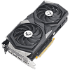
MSI GeForce RTX 3050 Gaming X Review
Test Setup »High-resolution PCB Pictures
These pictures are for the convenience of volt modders and people who would like to see all the finer details on the PCB. Feel free to link back to us and use these in your articles, videos or forum posts.
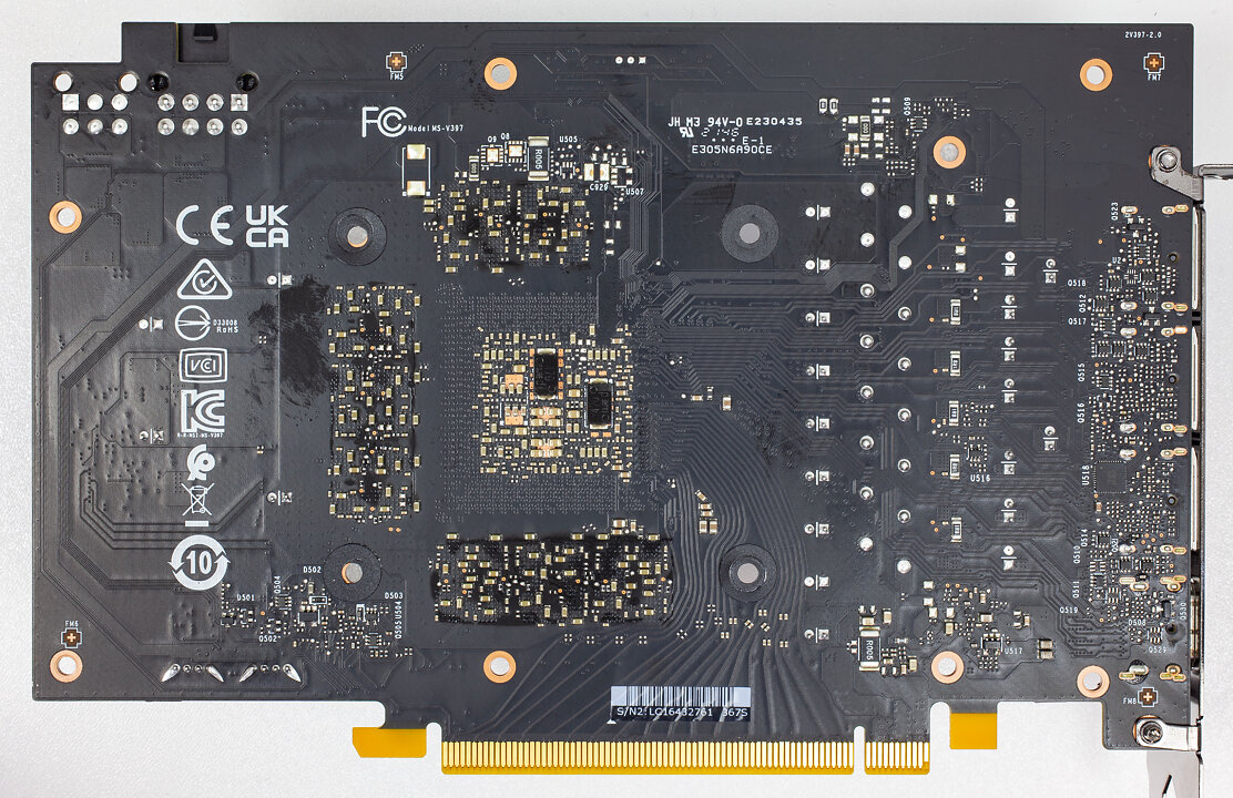
High-res versions are also available (front, back).
Circuit Board (PCB) Analysis
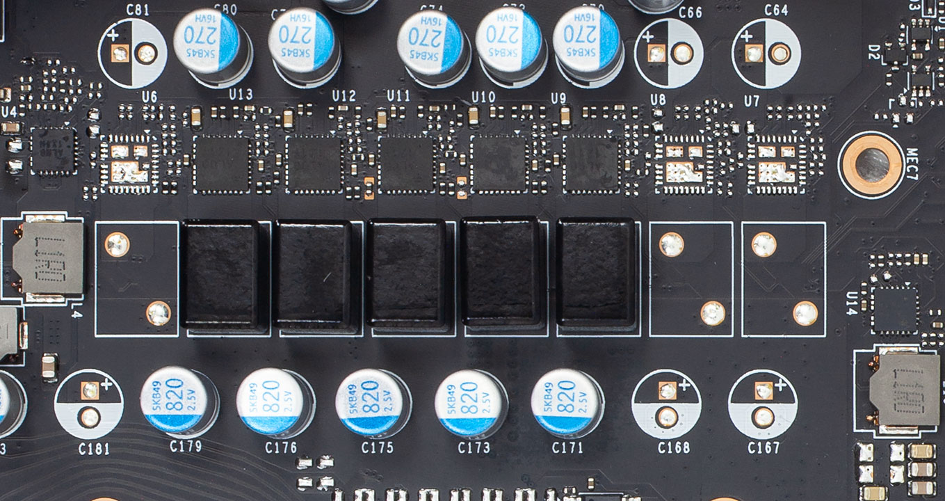
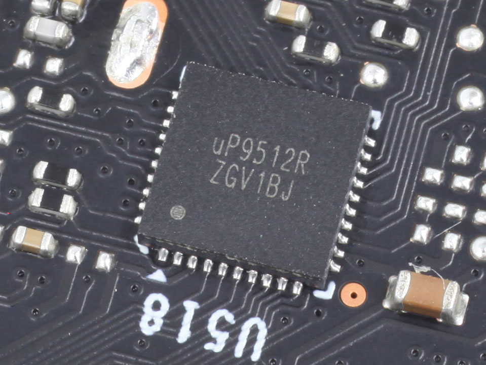
The GPU VRM is a five phase-design controlled by an uPI uP9512R controller.
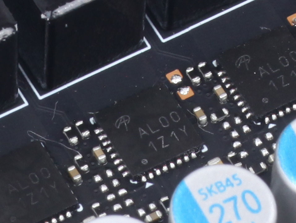
Alpha and Omega AOZ5332QI DrMOS chips are used for GPU voltage; they are rated for up to 50 A output current.
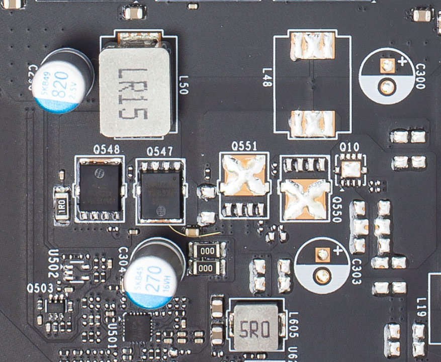
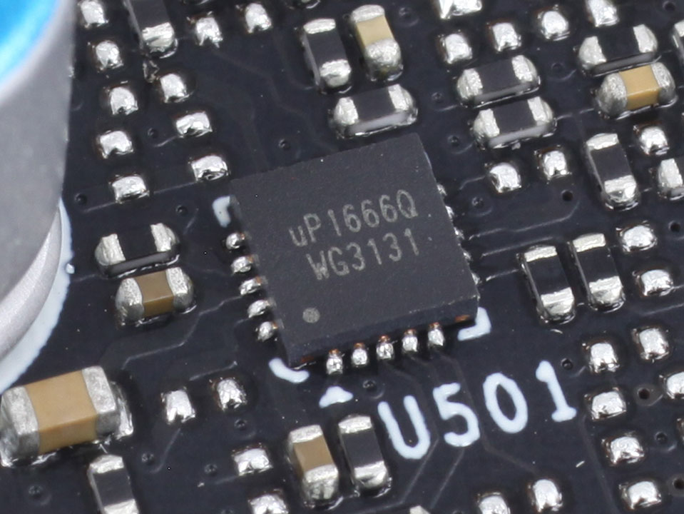
The memory VRM is single-phase and managed by a uPI uP1666Q controller.
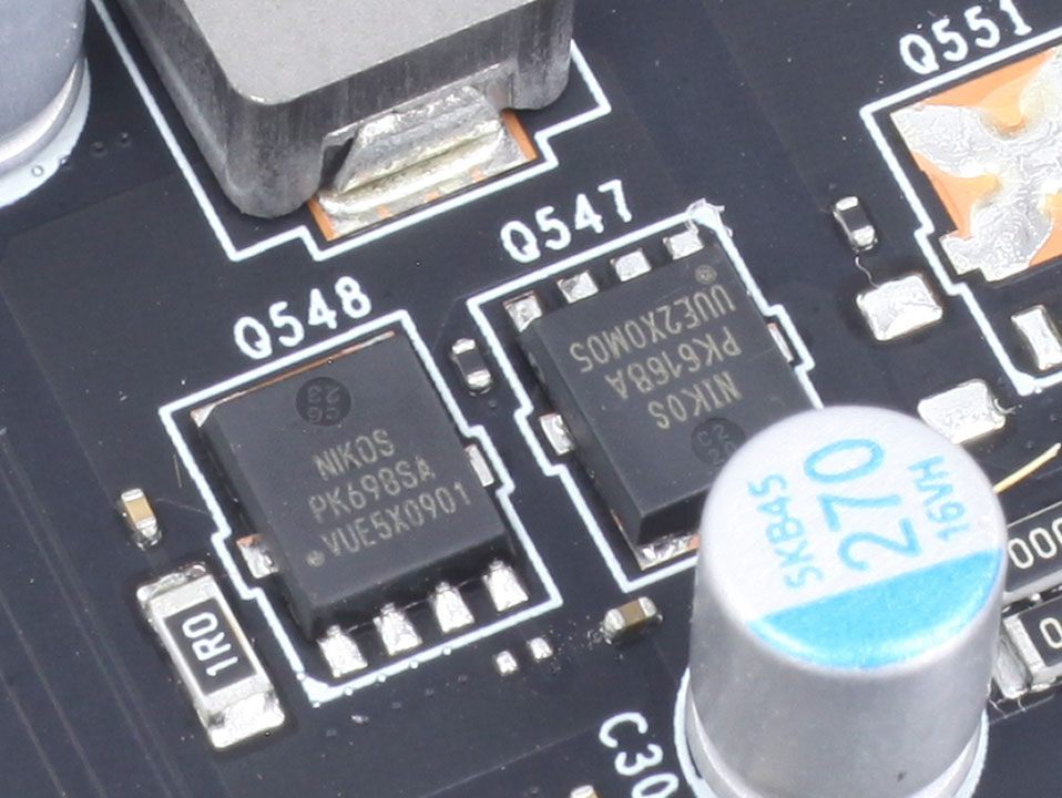
For memory, a classic dual MOSFET configuration is used, provided by Nikosem PK698SA and PK9168A, which are rated for 40 A.
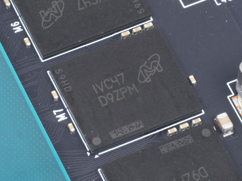
The GDDR6 memory chips are made by Micron and carry the model number D9ZPM, which decodes to MT61K512M32KPA-14:C. They are specified to run at 1750 MHz (14 Gbps GDDR6 effective).
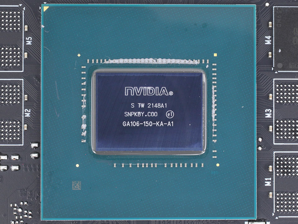
NVIDIA's GA106 graphics processor is made using Samsung's 8 nanometer node and has a transistor count of 12 billion with a die size of 276 mm².
Jul 12th, 2025 01:08 CDT
change timezone
Latest GPU Drivers
New Forum Posts
- 'NVIDIA App' not usable offline? (8)
- Can you guess Which game it is? (222)
- What are you playing? (23920)
- RX 9070 XT freezing/locking up only on desktop, anyone else? (43)
- NVIDIA RTX PRO 6000 Workstation Runs Much Hotter Than 5090 FE (22)
- Quick charging your USB devicesUSB 3.2 Gen 2x2 Type-C® front-panel. (1)
- GTX 1050 GPU Owners Club (12)
- ASUS ProArt GeForce RTX 4060 Ti OC Edition 16GB GDDR6 Gaming - nvflash64 VBIOS mismatch (2)
- Will you buy a RTX 5090? (640)
- No offense, here are some things that bother me about your understanding of fans. (33)
Popular Reviews
- Fractal Design Epoch RGB TG Review
- Corsair FRAME 5000D RS Review
- Lexar NM1090 Pro 4 TB Review
- NVIDIA GeForce RTX 5050 8 GB Review
- NZXT N9 X870E Review
- Sapphire Radeon RX 9060 XT Pulse OC 16 GB Review - An Excellent Choice
- AMD Ryzen 7 9800X3D Review - The Best Gaming Processor
- Upcoming Hardware Launches 2025 (Updated May 2025)
- Our Visit to the Hunter Super Computer
- Chieftec Iceberg 360 Review
TPU on YouTube
Controversial News Posts
- Intel's Core Ultra 7 265K and 265KF CPUs Dip Below $250 (288)
- Some Intel Nova Lake CPUs Rumored to Challenge AMD's 3D V-Cache in Desktop Gaming (140)
- AMD Radeon RX 9070 XT Gains 9% Performance at 1440p with Latest Driver, Beats RTX 5070 Ti (131)
- NVIDIA Launches GeForce RTX 5050 for Desktops and Laptops, Starts at $249 (119)
- NVIDIA GeForce RTX 5080 SUPER Could Feature 24 GB Memory, Increased Power Limits (115)
- Microsoft Partners with AMD for Next-gen Xbox Hardware (105)
- Intel "Nova Lake‑S" Series: Seven SKUs, Up to 52 Cores and 150 W TDP (100)
- NVIDIA DLSS Transformer Cuts VRAM Usage by 20% (97)