 111
111
MSI GeForce RTX 3090 Suprim X Review
Test Setup »High-resolution PCB Pictures
These pictures are for the convenience of volt modders and people who would like to see all the finer details on the PCB. Feel free to link back to us and use these in your articles or forum posts.

High-res versions are also available (front, back).
Circuit Board (PCB) Analysis
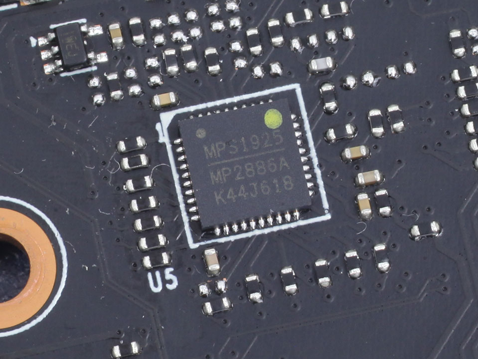
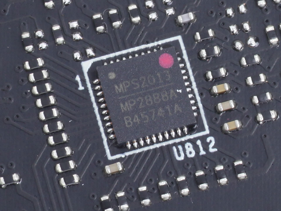
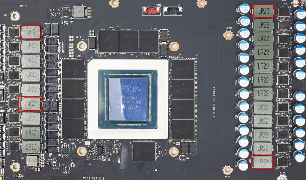
While the RTX 3080 Suprim uses a mixture of UPI and OnSemi controllers, the RTX 3090 variant is build around Monolithic Power Systems MPS controllers, which are slightly better, but more expensive.
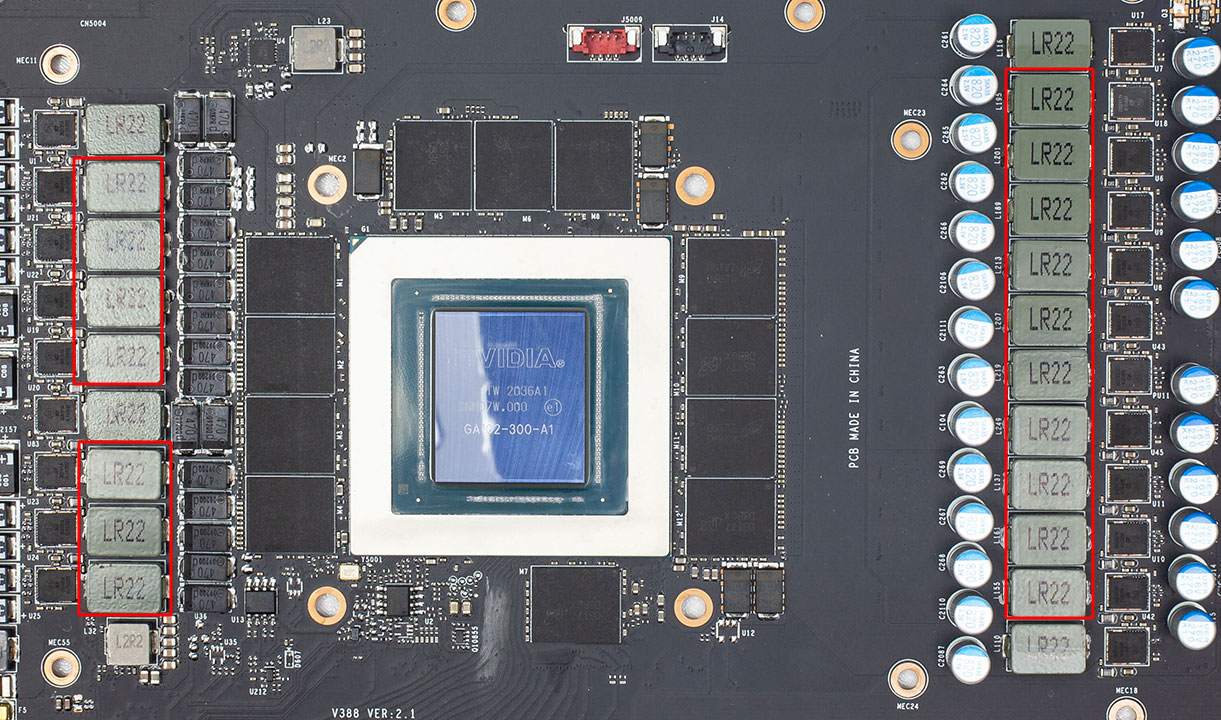
For GPU voltage, a 17-phase VRM configuration is installed, one more than on the RTX 3080.
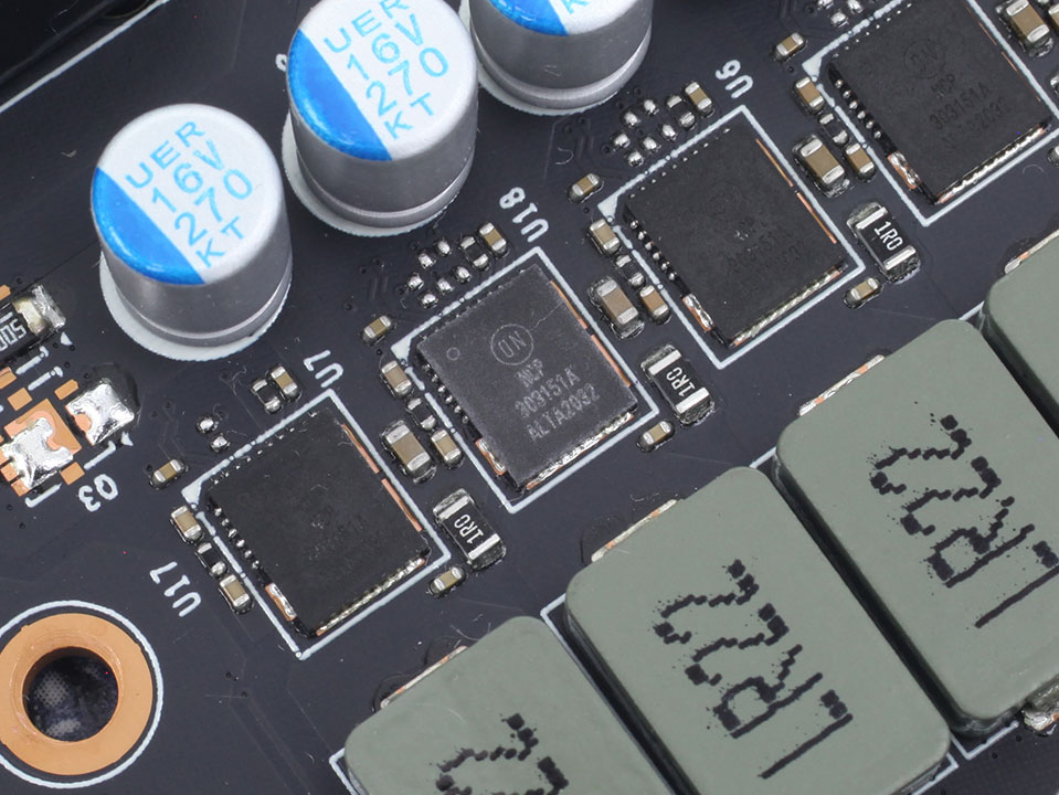
MSI is using OnSemi NCP303151A DrMOS chips throughout the VRM capable of 50 A.
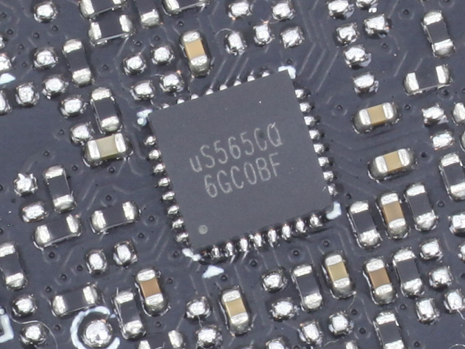
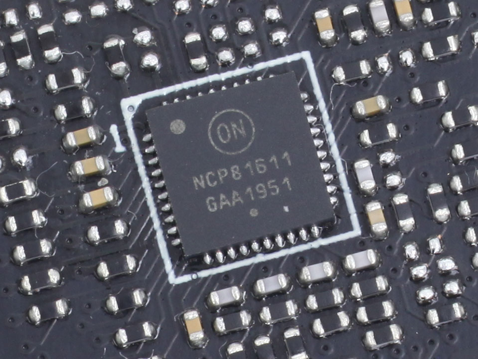
Memory voltage uses a 4-phase design and is generated by a UPI uS5650Q. Note the placement of the memory VRM phases—all spread out among the GPU power phases. The reason seems to be improved thermal performance and better voltage stability.
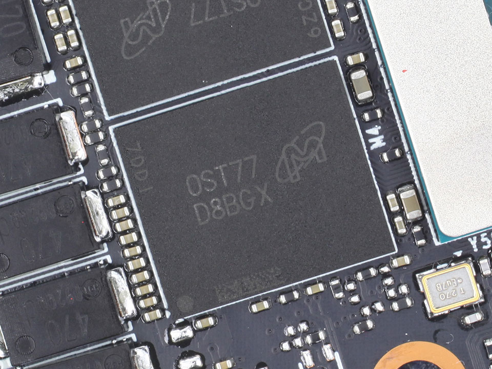
The GDDR6X memory chips are made by Micron and carry the model number D8BGX, which decodes to MT61K256M32JE-21. They are specified to run at 1313 MHz (21 Gbps GDDR6X effective).
GDDR6X doubles the data rate once again over GDDR6. It no longer transmits one bit of information by setting the voltage to either "on" or "off," but instead sends two bits of information at the same time by using four different voltage levels.
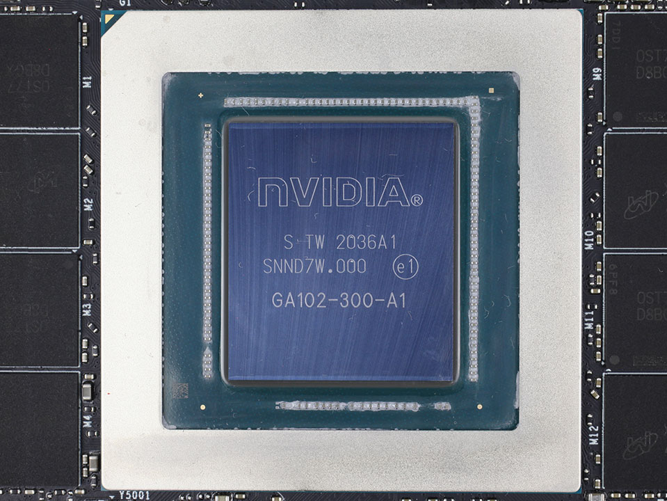
NVIDIA's GA102 graphics processor is the company's second Ampere architecture chip; the first one targeted at GeForce gamers. It is produced on a 8 nanometer process at Samsung and has a transistor count of 28 billion with a die size of 628 mm².
Jul 18th, 2025 19:19 CDT
change timezone
Latest GPU Drivers
New Forum Posts
- Anime Nation (13052)
- What's your latest tech purchase? (24305)
- AI Job Losses: let's count the losses up, total losses to AI so far 94,000 and counting (35)
- lower score 5070Ti after replacing the PSU (0)
- TPU's Nostalgic Hardware Club (20539)
- 3DMARK "LEGENDARY" (329)
- Hatsune Miku x ASUS TUF Gaming Build (67)
- Ferrari themed mod cont. 4070s repaste (7)
- Stalker 2 is looking great. (213)
- Share your CPU-X Benchmarks! (6)
Popular Reviews
- MSI GeForce RTX 5060 Gaming OC Review
- Razer Blade 16 (2025) Review - Thin, Light, Punchy, and Efficient
- Thermal Grizzly WireView Pro Review
- Pulsar X2 Crazylight Review
- SilverStone SETA H2 Review
- AVerMedia Live Gamer Ultra S (GC553Pro) Review
- Upcoming Hardware Launches 2025 (Updated May 2025)
- Sapphire Radeon RX 9060 XT Pulse OC 16 GB Review - An Excellent Choice
- NVIDIA GeForce RTX 5050 8 GB Review
- Our Visit to the Hunter Super Computer
TPU on YouTube
Controversial News Posts
- Intel's Core Ultra 7 265K and 265KF CPUs Dip Below $250 (288)
- Some Intel Nova Lake CPUs Rumored to Challenge AMD's 3D V-Cache in Desktop Gaming (140)
- AMD Radeon RX 9070 XT Gains 9% Performance at 1440p with Latest Driver, Beats RTX 5070 Ti (131)
- NVIDIA Launches GeForce RTX 5050 for Desktops and Laptops, Starts at $249 (124)
- NVIDIA GeForce RTX 5080 SUPER Could Feature 24 GB Memory, Increased Power Limits (115)
- Microsoft Partners with AMD for Next-gen Xbox Hardware (105)
- NVIDIA DLSS Transformer Cuts VRAM Usage by 20% (99)
- AMD Sampling Next-Gen Ryzen Desktop "Medusa Ridge," Sees Incremental IPC Upgrade, New cIOD (97)