 11
11
MSI GeForce RTX 4060 Ti Gaming X Trio Review
Test Setup »High-resolution PCB Pictures
These pictures are for the convenience of volt modders and people who would like to see all the finer details on the PCB. Feel free to link back to us and use these in your articles, videos or forum posts.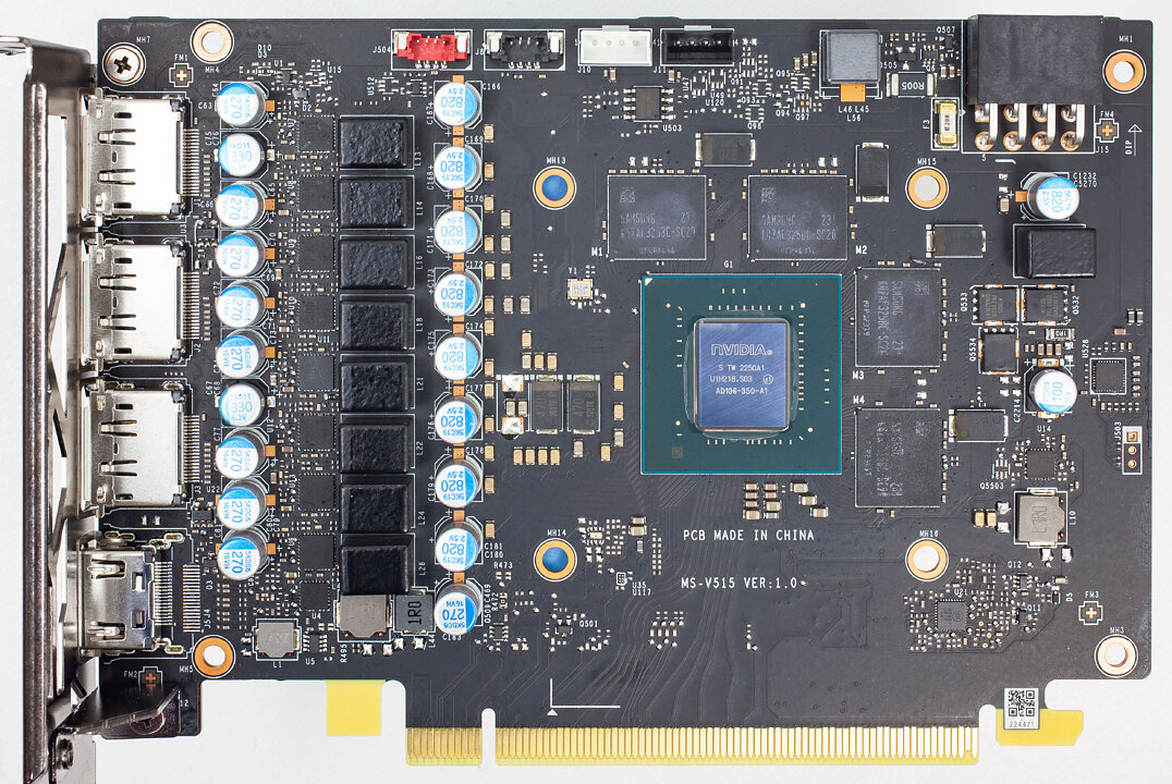
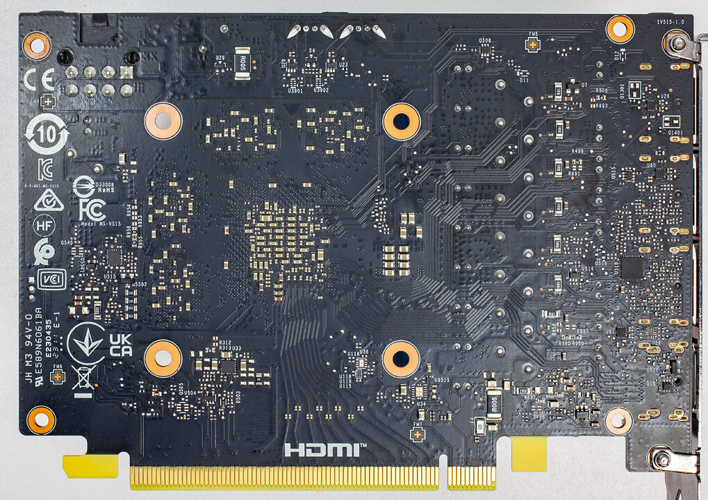
High-resolution versions are also available (front, back).
Circuit Board (PCB) Analysis
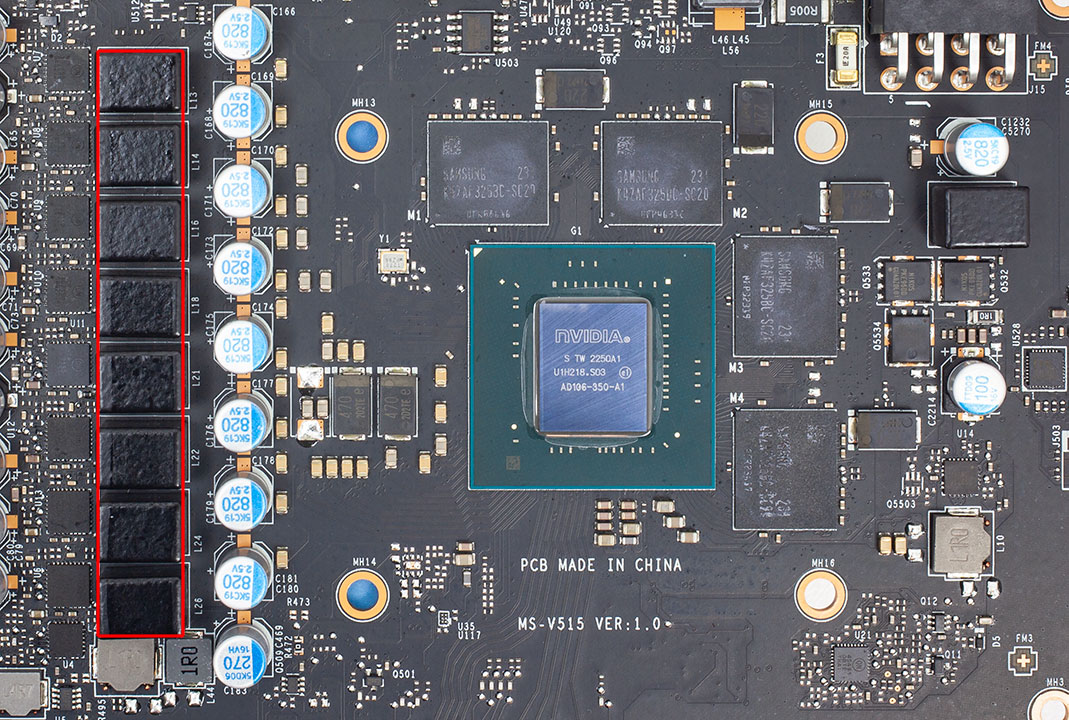

GPU voltage is handled by an 8-phase VRM that's controlled by a UPI uP9512R controller.
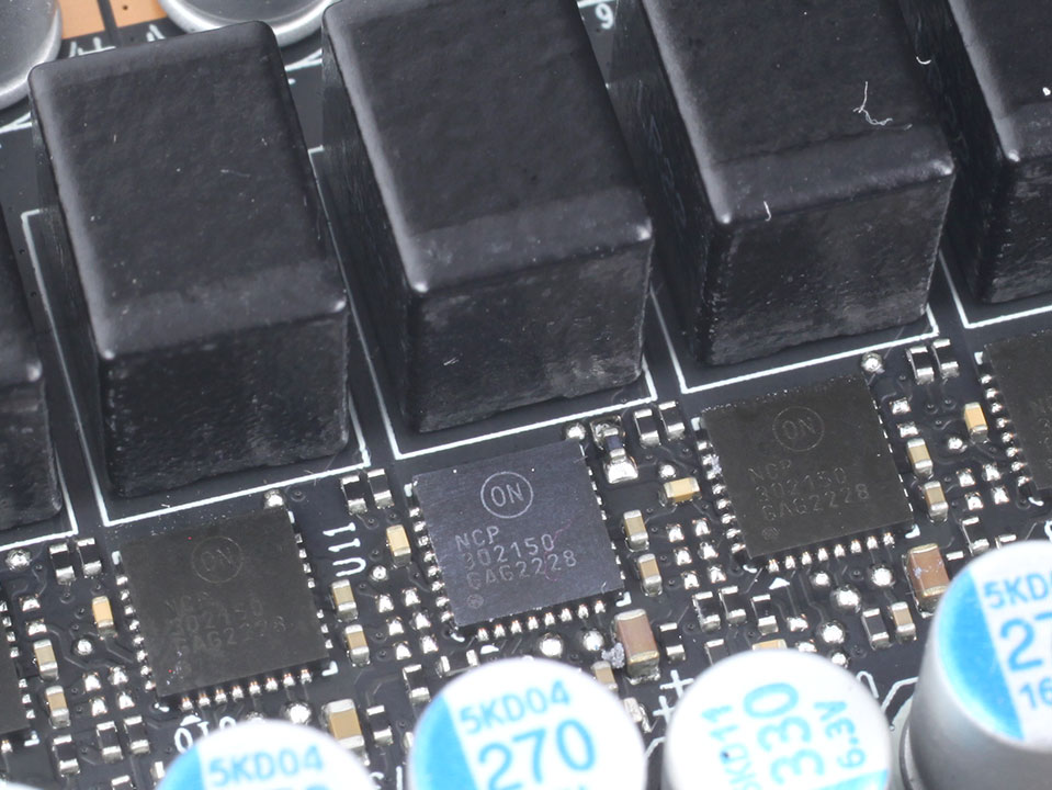
OnSemi NCP302150 DrMOS components are used for GPU voltage; they are rated for 50 A of current each.

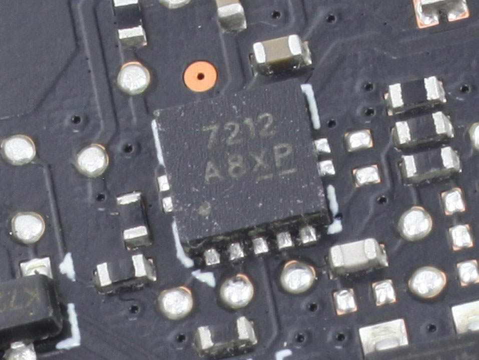
Memory voltage is a single-phase design, and handled by a 7212 buck controller.
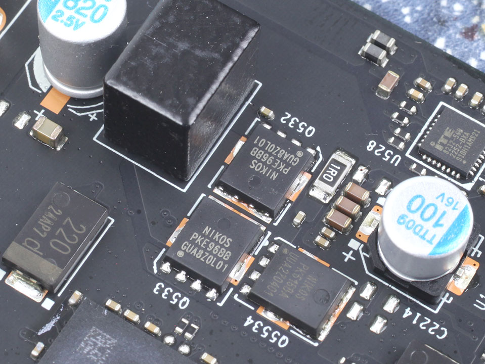
For memory, MSI is using a set of Nikos PKE96BB discrete MOSFETs rated for 50 A.
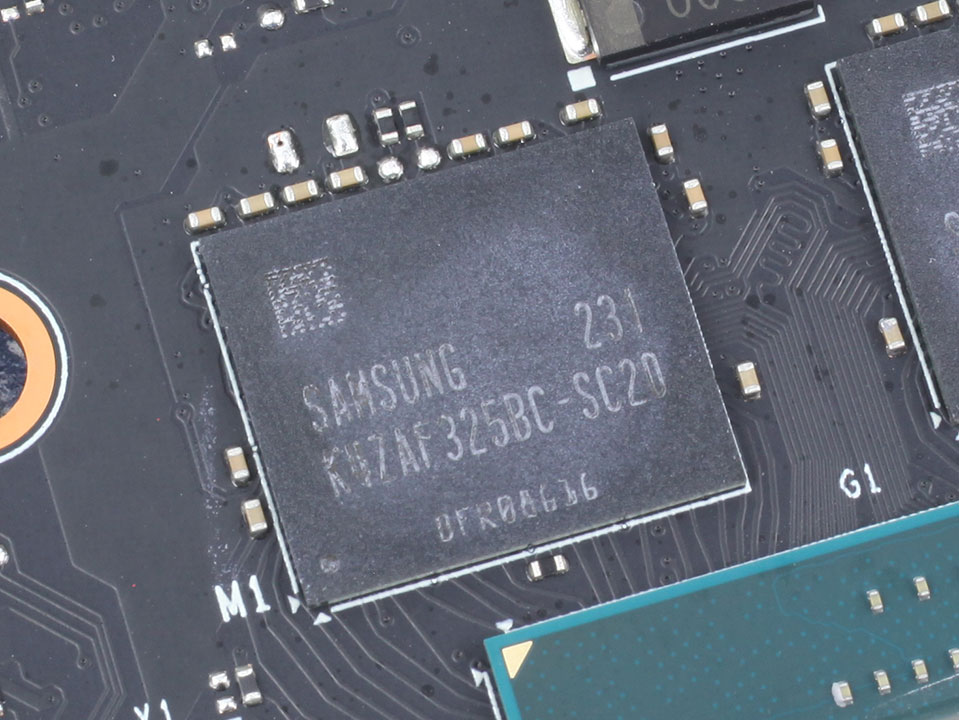
The memory chips are Samsung K4ZAF325BC-SC20, these are 20 Gbps-rated GDDR6 memory chips.
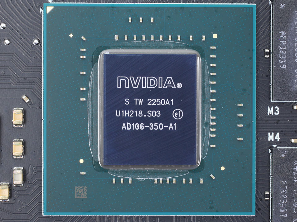
NVIDIA's AD106 graphics processor is the company's fourth Ada Lovelace GPU. It is built using a 5 nanometer process at TSMC Taiwan, with a transistor count of 22.9 billion and a die size of 190 mm².
Jul 12th, 2025 07:37 CDT
change timezone
Latest GPU Drivers
New Forum Posts
- Gigabyte graphic cards - TIM gel SLIPPAGE problem (147)
- Will you buy a RTX 5090? (647)
- 5070 Ti Variants, do they even matter? (20)
- 'NVIDIA App' not usable offline? (10)
- Chrome has removed uBlock Origin 1.64.0 (remove google search suggestions) (8)
- Gpu overheating after bios flash (2)
- What's your latest tech purchase? (24242)
- 3D Printer Club (540)
- Can you guess Which game it is? (230)
- Is RX 9070 VRAM temperature regular value or hotspot? (401)
Popular Reviews
- Fractal Design Epoch RGB TG Review
- Lexar NM1090 Pro 4 TB Review
- Corsair FRAME 5000D RS Review
- NVIDIA GeForce RTX 5050 8 GB Review
- NZXT N9 X870E Review
- Our Visit to the Hunter Super Computer
- Sapphire Radeon RX 9060 XT Pulse OC 16 GB Review - An Excellent Choice
- AMD Ryzen 7 9800X3D Review - The Best Gaming Processor
- Upcoming Hardware Launches 2025 (Updated May 2025)
- Chieftec Iceberg 360 Review
TPU on YouTube
Controversial News Posts
- Intel's Core Ultra 7 265K and 265KF CPUs Dip Below $250 (288)
- Some Intel Nova Lake CPUs Rumored to Challenge AMD's 3D V-Cache in Desktop Gaming (140)
- AMD Radeon RX 9070 XT Gains 9% Performance at 1440p with Latest Driver, Beats RTX 5070 Ti (131)
- NVIDIA Launches GeForce RTX 5050 for Desktops and Laptops, Starts at $249 (119)
- NVIDIA GeForce RTX 5080 SUPER Could Feature 24 GB Memory, Increased Power Limits (115)
- Microsoft Partners with AMD for Next-gen Xbox Hardware (105)
- Intel "Nova Lake‑S" Series: Seven SKUs, Up to 52 Cores and 150 W TDP (100)
- NVIDIA DLSS Transformer Cuts VRAM Usage by 20% (97)