 297
297
NVIDIA GeForce RTX 5070 Founders Edition Review
Neural Rendering, DLSS 4, Reflex 2 »NVIDIA Blackwell Architecture
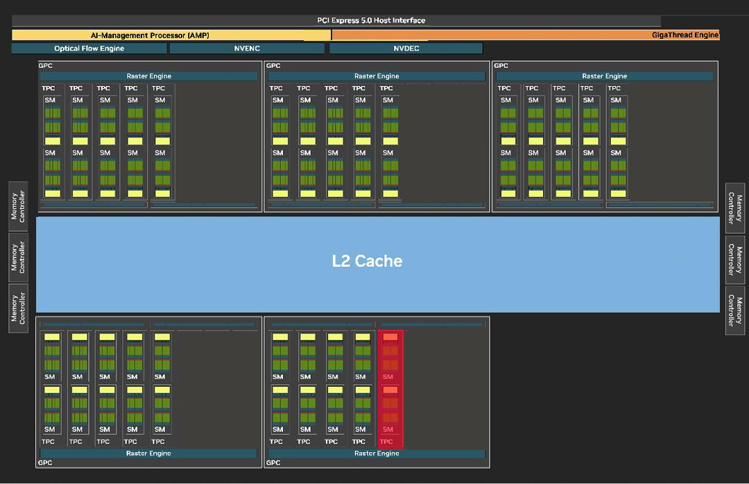
NVIDIA does not provide a block diagram for the GB205 GPU (we asked), so we had to quickly hack one out from the GB202 diagram. This is accurate just not as pretty.
The GeForce Blackwell graphics architecture heralds NVIDIA's 4th generation of RTX, the late-2010s re-invention of the modern GPU that sees a fusion of real time ray traced objects with conventional raster 3D graphics. With Blackwell, NVIDIA is helping add another dimension, neural rendering, the ability for the GPU to leverage a generative AI to create portions of a frame. This is different from DLSS, where an AI model is used to reconstruct details in an upscaled frame based on its training date, temporal frames, and motion vectors. Today we are reviewing NVIDIA's fourth GPU from this generation, the RTX 5070. At the heart of this graphics card is the new 5 nm GB205 silicon. This chip has a unique die-size and SM count that doesn't have a predecessor from the previous Ada generation. NVIDIA skipped a direct successor to the AD104 in the Blackwell generation, instead building the RTX 5070 Ti on the larger GB203 silicon and the RTX 5070 on the technically smaller GB205. The chip measures 263 mm² in die-area, with a transistor count of 31.1 billion, both of which are smaller than those of the AD104, which had to part with nearly a fifth of its shaders to yield an RTX 4070. Given its volumes, NVIDIA would probably have had to part with perfectly good AD104 chips to carve out the RTX 4070. It's to minimize this die area wastage in this generation that the company set out to create the GB205.
The GB205 silicon is laid out essentially in the same component hierarchy as past generations of NVIDIA GPUs, but with a few notable changes. The GPU features a PCI-Express 5.0 x16 host interface. PCIe Gen 5 has been around since Intel's 12th Gen Core "Alder Lake" and AMD's Ryzen 7000 "Zen 4," so there is a sizable install-base of systems that can take advantage of it. The GPU is of course compatible with older generations of PCIe. The GB205 also features the new GDDR7 memory interface that's making its debut with this generation. The chip features a 192-bit wide memory bus. NVIDIA is using this to drive 12 GB of memory at 28 Gbps speeds, yielding 672 GB/s of memory bandwidth, which is a 33% increase over the RTX 4070 and its 21 Gbps GDDR6X.
The GigaThread Engine is the main graphics rendering workload allocation logic on the GB205, but there's a new addition, a dedicated serial processor for managing all AI acceleration resources on the GPU, NVIDIA calls this AMP (AI management processor). Other components at the global level are the Optical Flow Processor, a component involved in older versions of DLSS frame generation and for video encoding; and an updated media acceleration engine consisting of one each of NVDEC and NVENC video accelerators. The new 9th Gen NVENC video encode accelerators come with 4:2:2 AV1 and HEVC encoding support. The central region of the GPU has the single largest common component, the 48 MB L2 cache, which the RTX 5070 maxes out. This is an increase over the 36 MB that the RTX 4070 has.
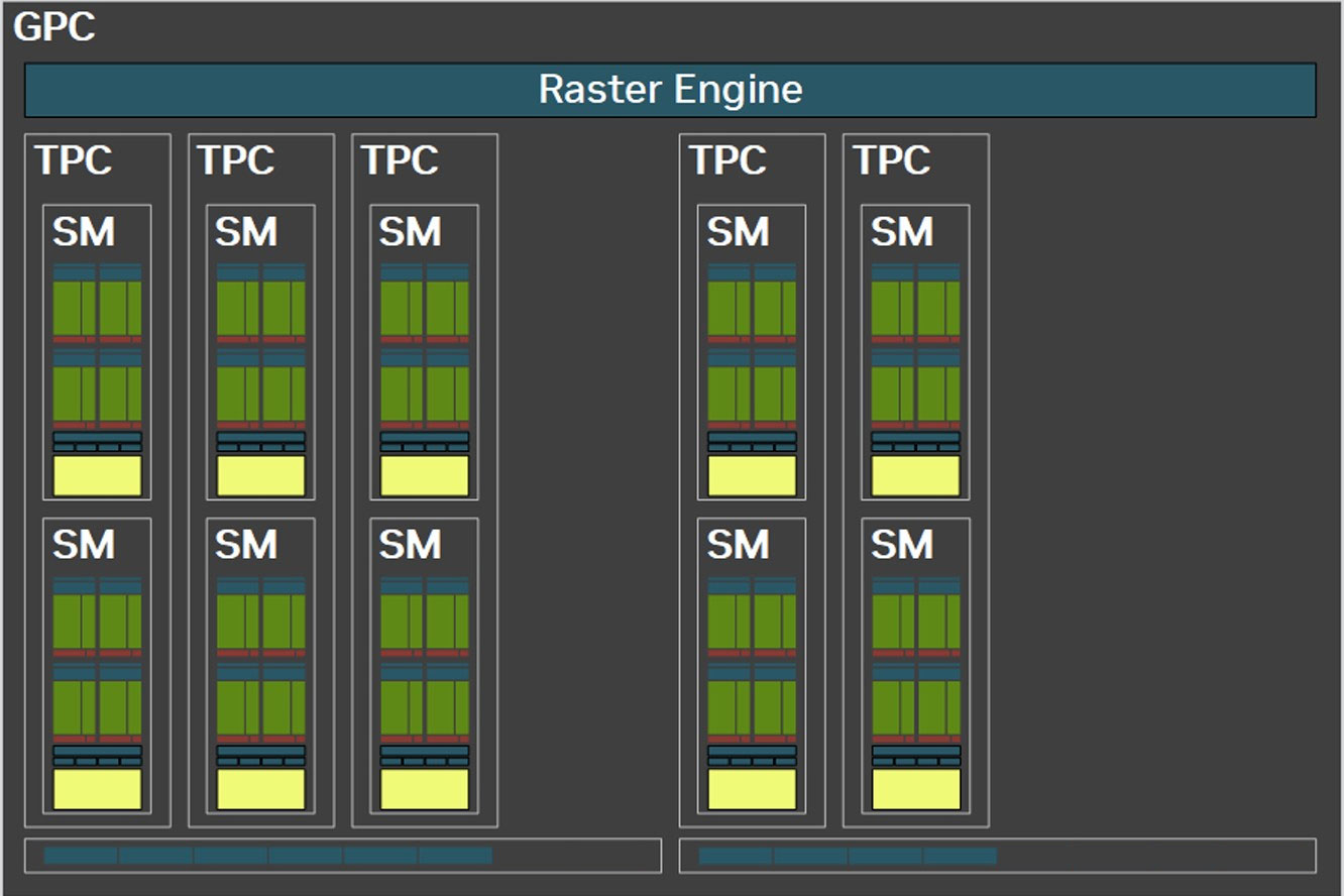
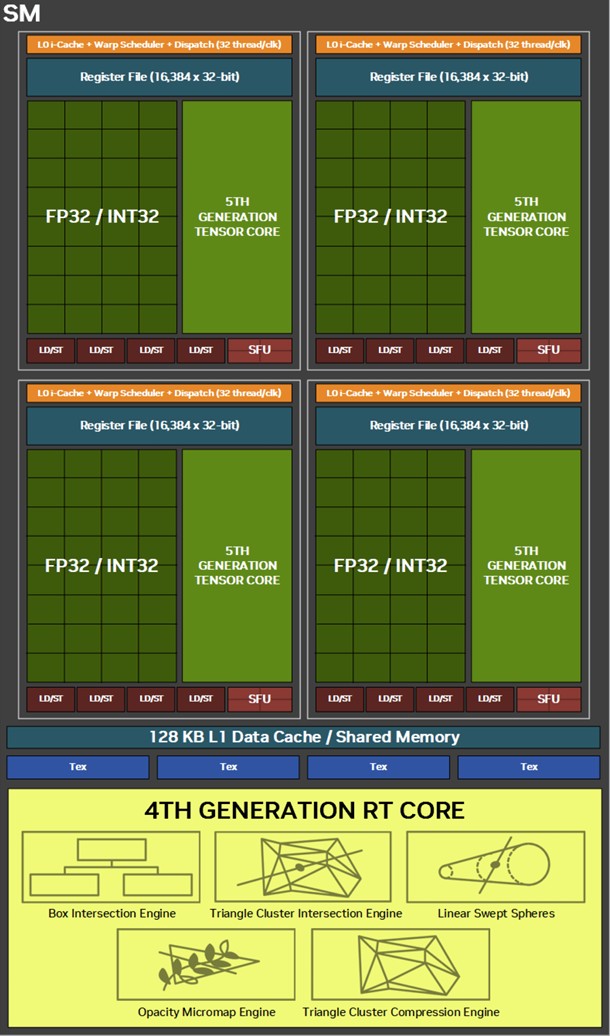
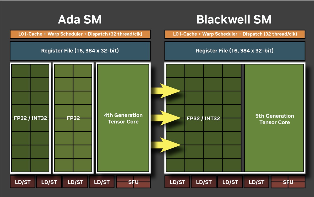
There are five graphics processing clusters (GPC) on the GB205. Each of these contains 10 streaming multiprocessors (SM) across 5 texture processing clusters (TPCs), and a raster engine consisting of 16 ROPs. Each SM contains 128 CUDA cores. Unlike the Ada generation SM that each had 64 FP32+INT32 and 64 purely-FP32 SIMD units, the new Blackwell generation SM features concurrent FP32+INT32 capability on all 128 SIMD units. These 128 CUDA cores are arranged in four slices, each with a register file, a level-0 instruction cache, a warp scheduler, two sets of load-store units, and a special function unit (SFU) handling some special math functions such as trigonometry, exponents, logarithms, reciprocals, and square-root. The four slices share a 128 KB L1 data cache, and four TMUs. The most exotic components of the Blackwell SM are the four 5th Gen Tensor cores, and a 4th Gen RT core.
With 5 GPCs containing 5 TPCs each, there are a total of 50 SM, worth 6,400 CUDA cores, 200 Tensor cores, 50 RT cores, and 200 TMUs, on the GB205 silicon. The RTX 5070 doesn't max out the silicon, it gets 48 out of the 50 SM, resulting in 6,144 CUDA cores, 192 Tensor cores, 48 RT cores, and 192 TMUs. The GB205 silicon is endowed with 80 ROPs, all of which are enabled on the RTX 5070. This is a step up from the RTX 4070, which only had 64 out of 80 ROPs present on the AD104 silicon. The RTX 5070 also maxes out all 48 MB of L2 cache present on the die, while the RTX 4070 only had 36 MB out of the 48 MB present.
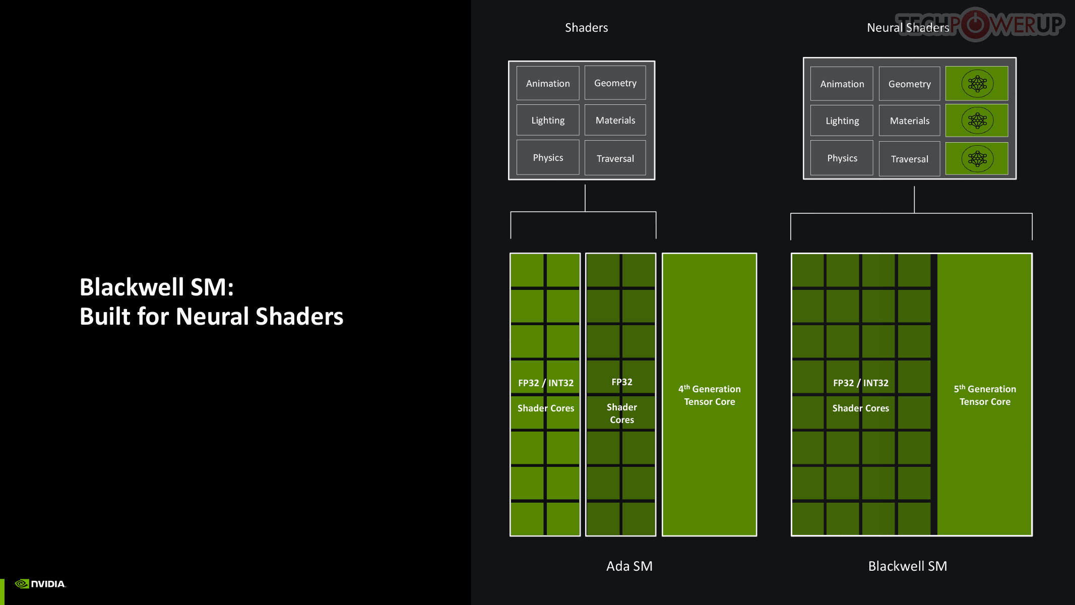
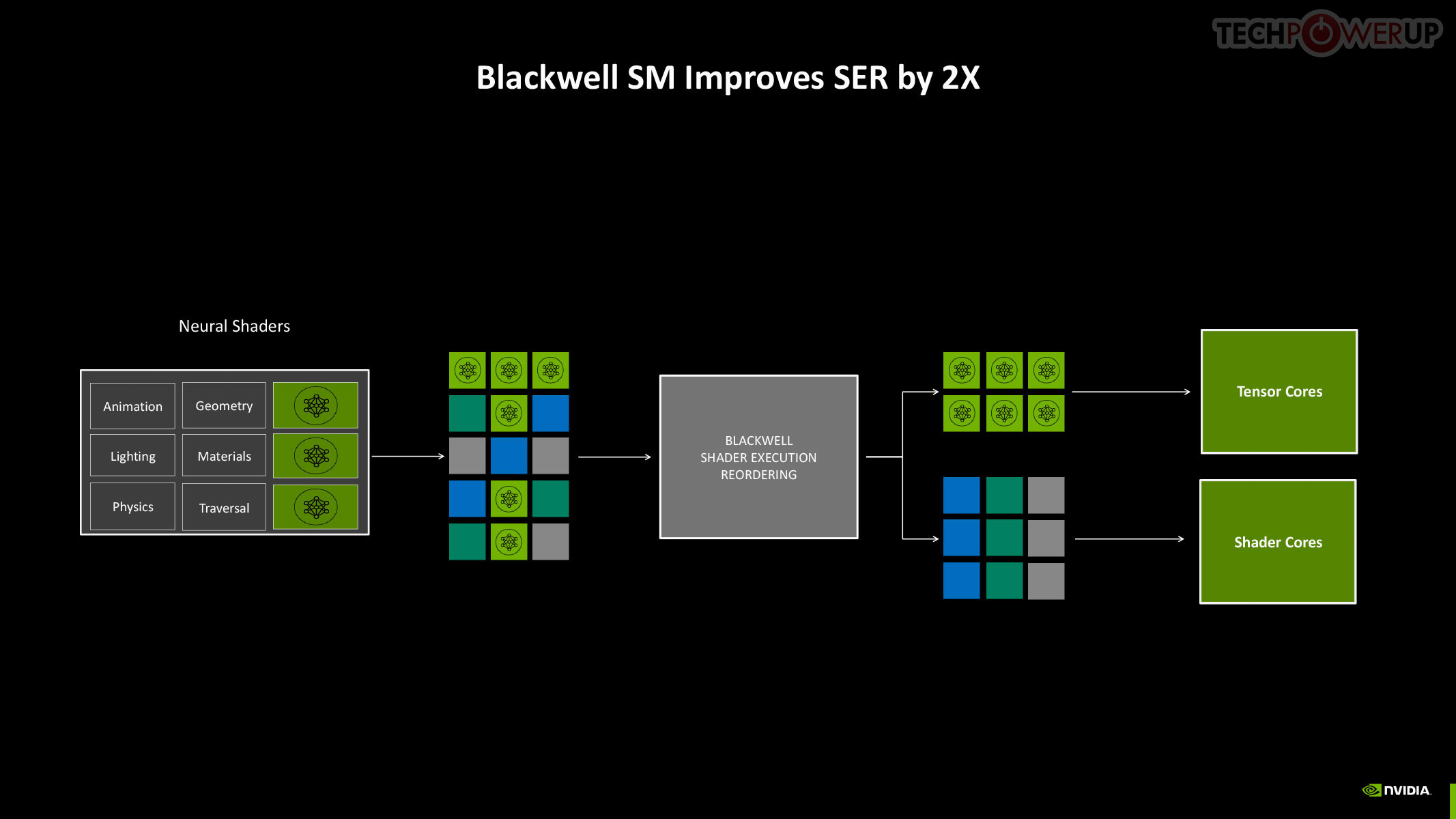
Perhaps the biggest change to the way the SM handles work introduced with Blackwell is the concept of neural shaders—treating portions of the graphics rendering workload done by a generative AI model as shaders. Microsoft has laid the groundwork for standardization of neural shaders with its Cooperative Vectors API, in the latest update to DirectX 12. The Tensor cores are now accessible for workloads through neural shaders, and the shader execution reordering (SER) engine of the Blackwell SM is able to more accurately reorder workloads for the CUDA cores and the Tensor core in an SM.
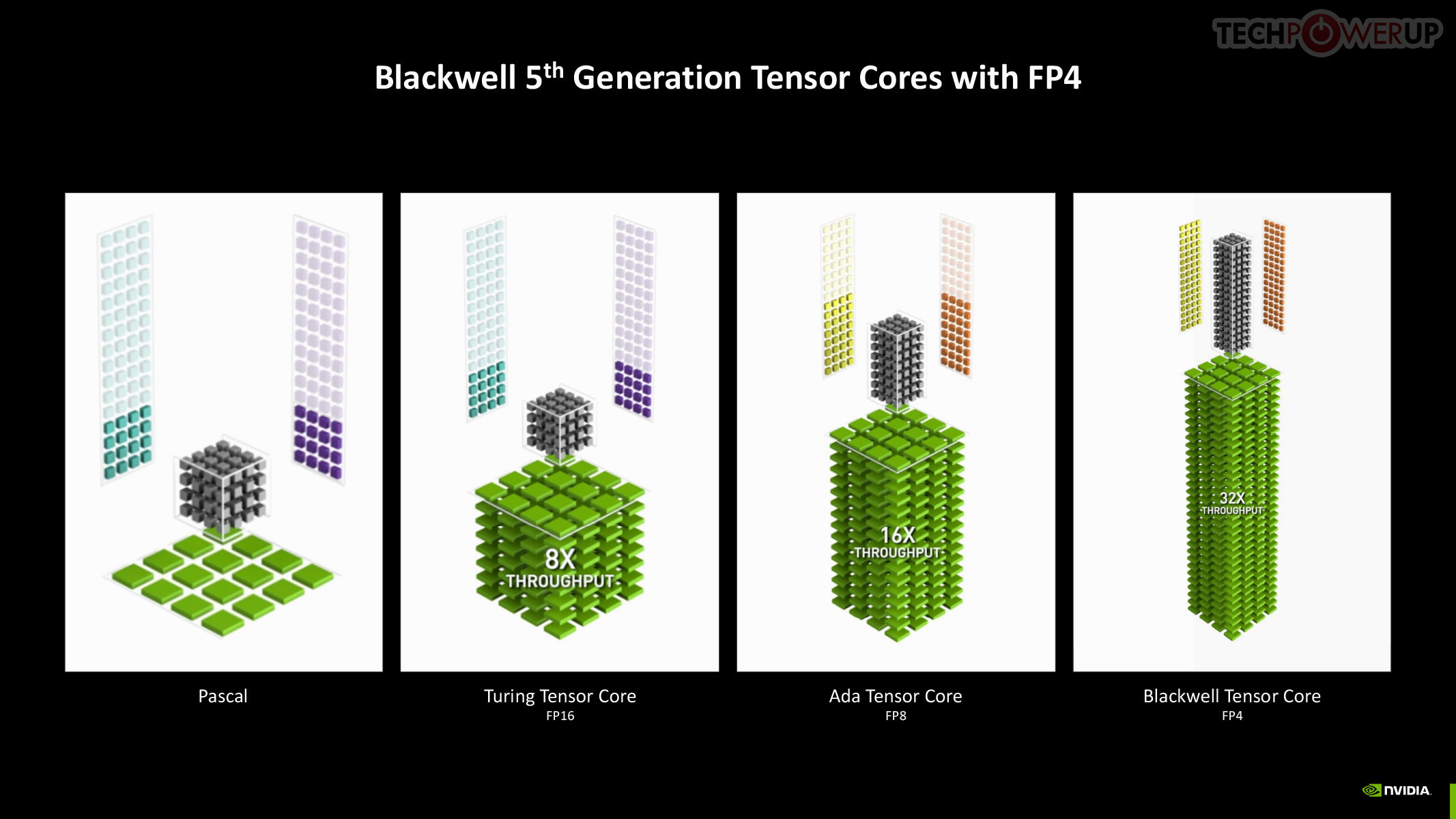
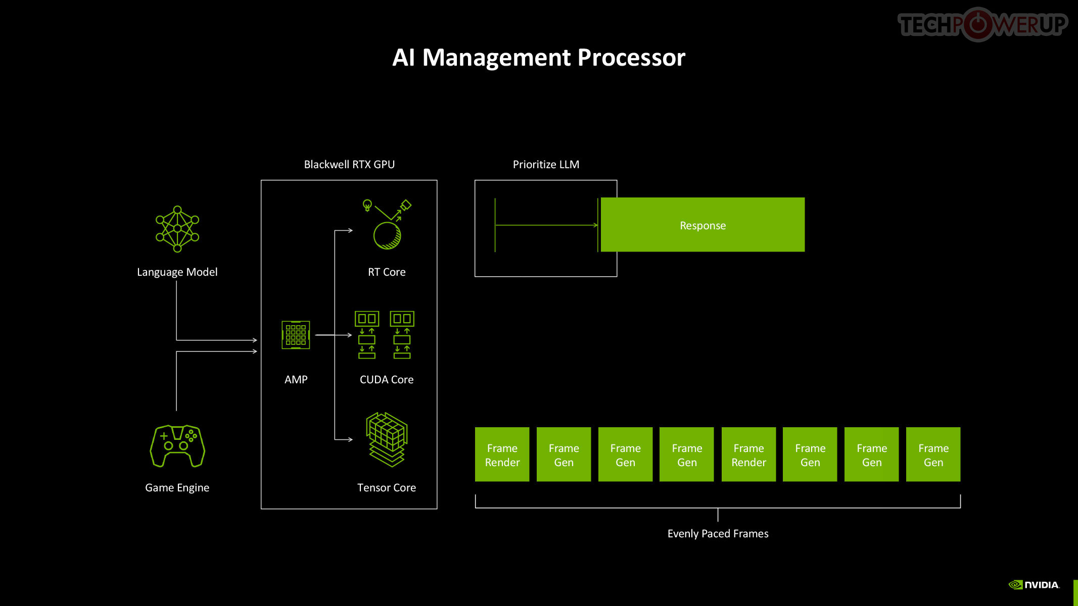
The new 5th Gen Tensor core introduces support for FP4 data format (1/8 precision) to fast moving atomic workloads, providing 32 times the throughput of the very first Tensor core introduced with the Volta architecture. Over the generations, AI models leveraged lesser precision data formats, and sparsity, to improve performance. The AI management processor (AMP) is what enables simultaneous AI and graphics workloads at the highest levels of the GPU, so it could be simultaneously rendering real time graphics for a game, while running an LLM, without either affecting the performance of the other. AMP is a specialized hardware scheduler for all the AI acceleration resources on the silicon. This plays a crucial role for DLSS 4 multi-frame generation to work.
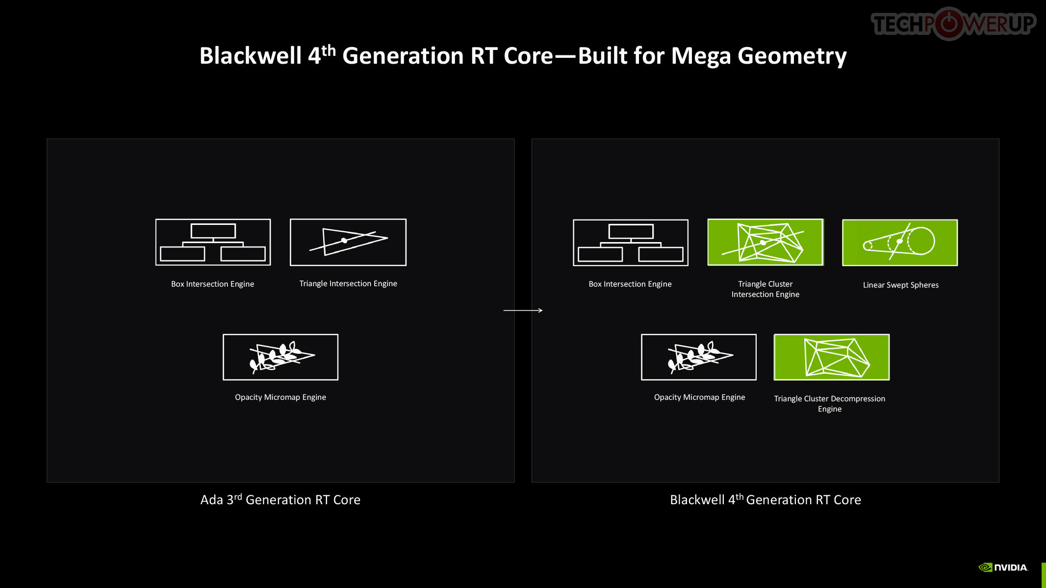
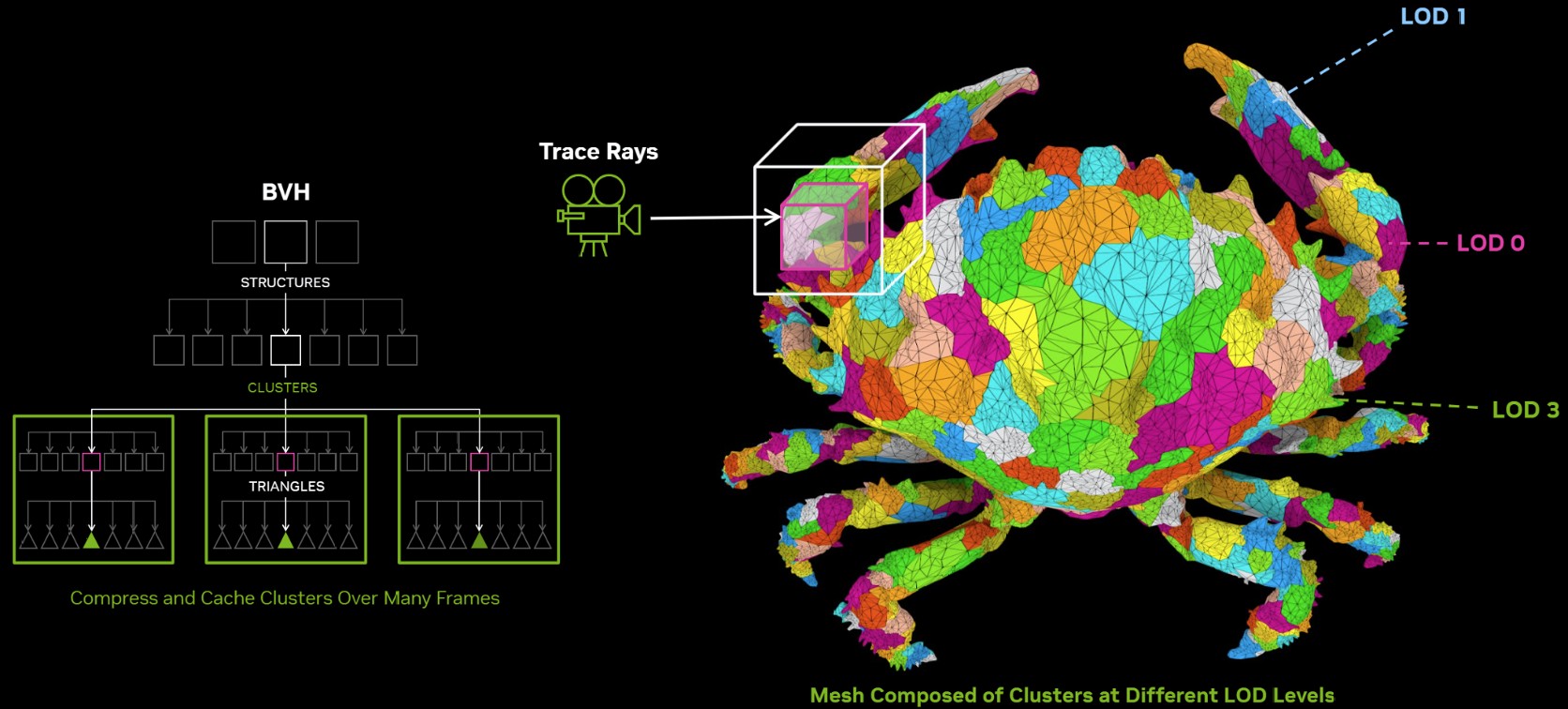
The 4th Gen RT core not just offers a generational increase in ray testing and ray intersection performance, which lowers the performance cost of enabling path tracing and ray traced effects; but also offers a potential generational leap in performance with the introduction of Mega Geometry. This allows for ray traced objects with extremely high polygon counts, increasing their detail. Poly count and ray tracing present linear increases in performance costs, as each triangle has to intersect with a ray, and there should be sufficient rays to intersect with each of them. This is achieved by adopting clusters of triangles in an object as first-class primitives, and cluster-level acceleration structures. The new RT cores introduce a component called a triangle cluster intersection engine, designed specifically for handling mega geometry. The integration of a triangle cluster compression format and a lossless decompression engine allows for more efficient processing of complex geometry.
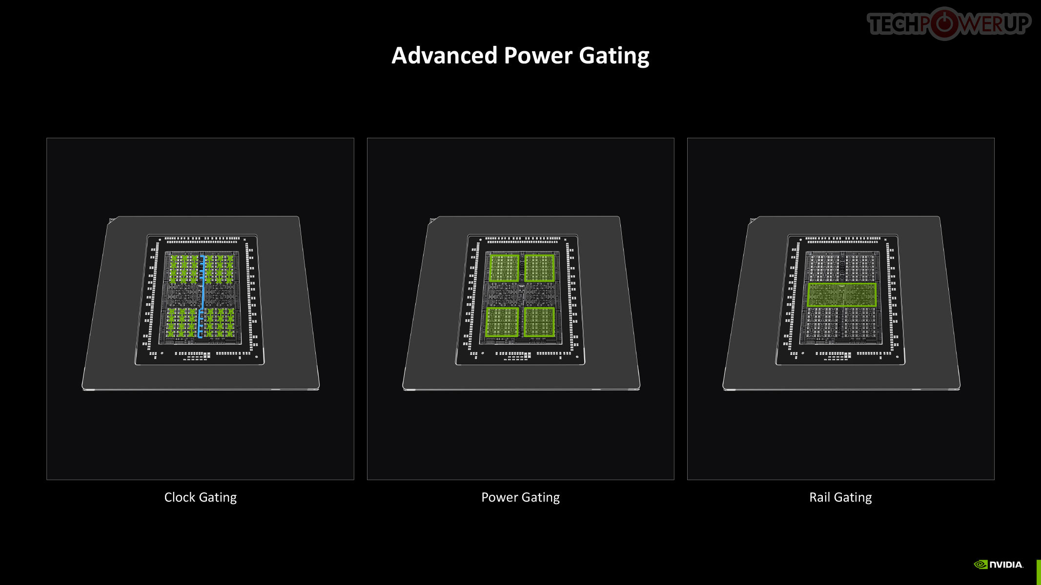
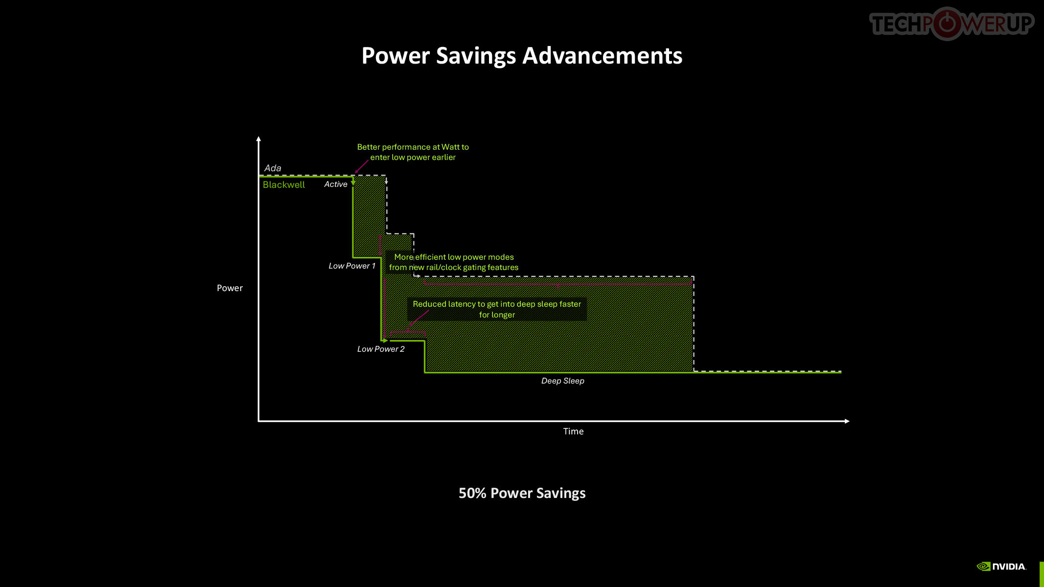
The GB205 and the rest of the GeForce Blackwell GPU family is built on the exact same TSMC "NVIDIA 4N" foundry node, which is actually 5 nm, as previous-generation Ada, so NVIDIA directed efforts to finding innovative new ways to manage power and thermals. This is done through a re-architected power management engine that relies on clock gating, power gating, and rail gating of the individual GPCs and other top-level components. It also worked on the speed at which the GPU makes power-related decisions.
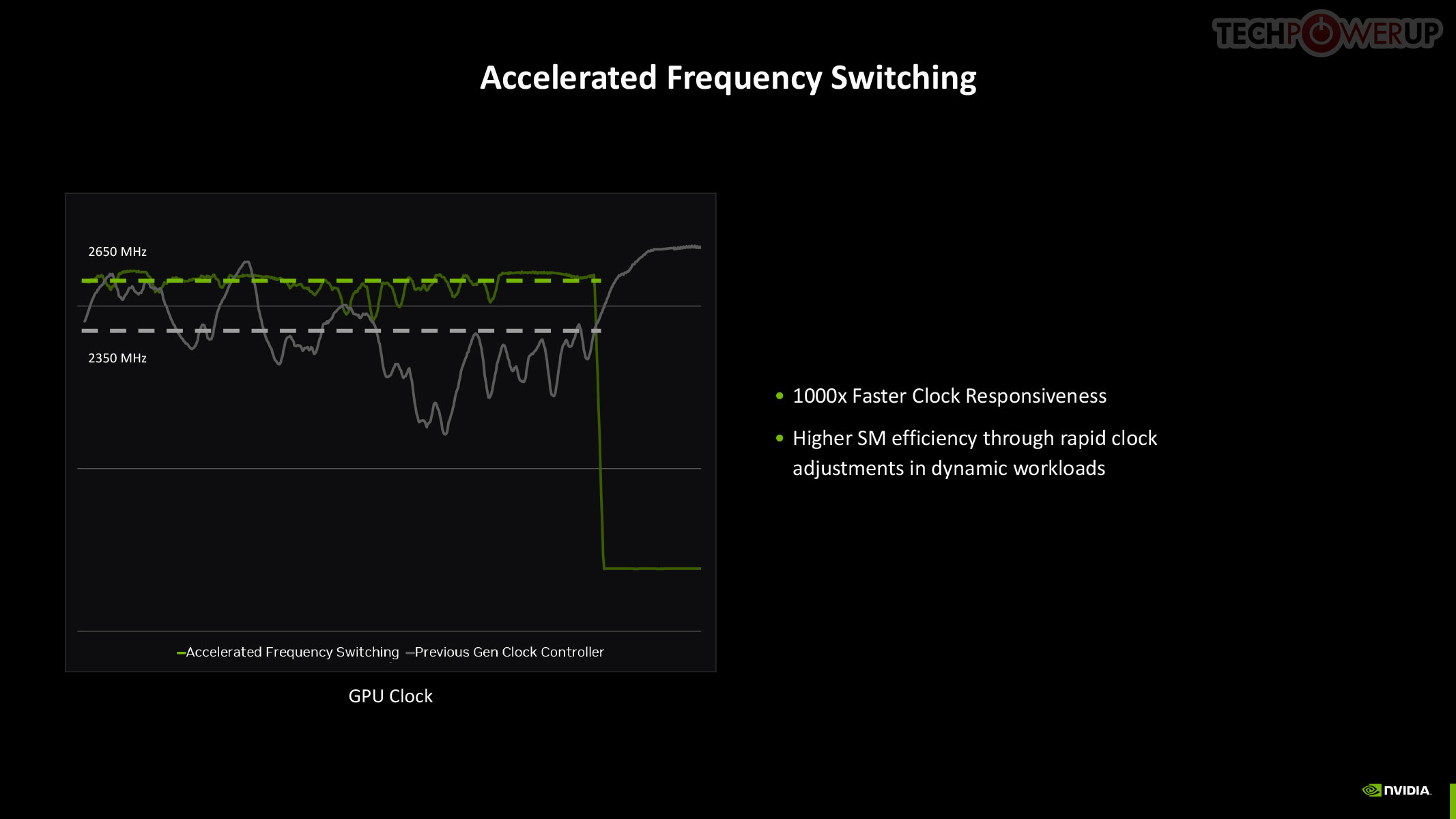
The quickest way to drop power is by adjusting the GPU clock speed, and with Blackwell, NVIDIA introduced a means for rapid clock adjustments at the SM-level.
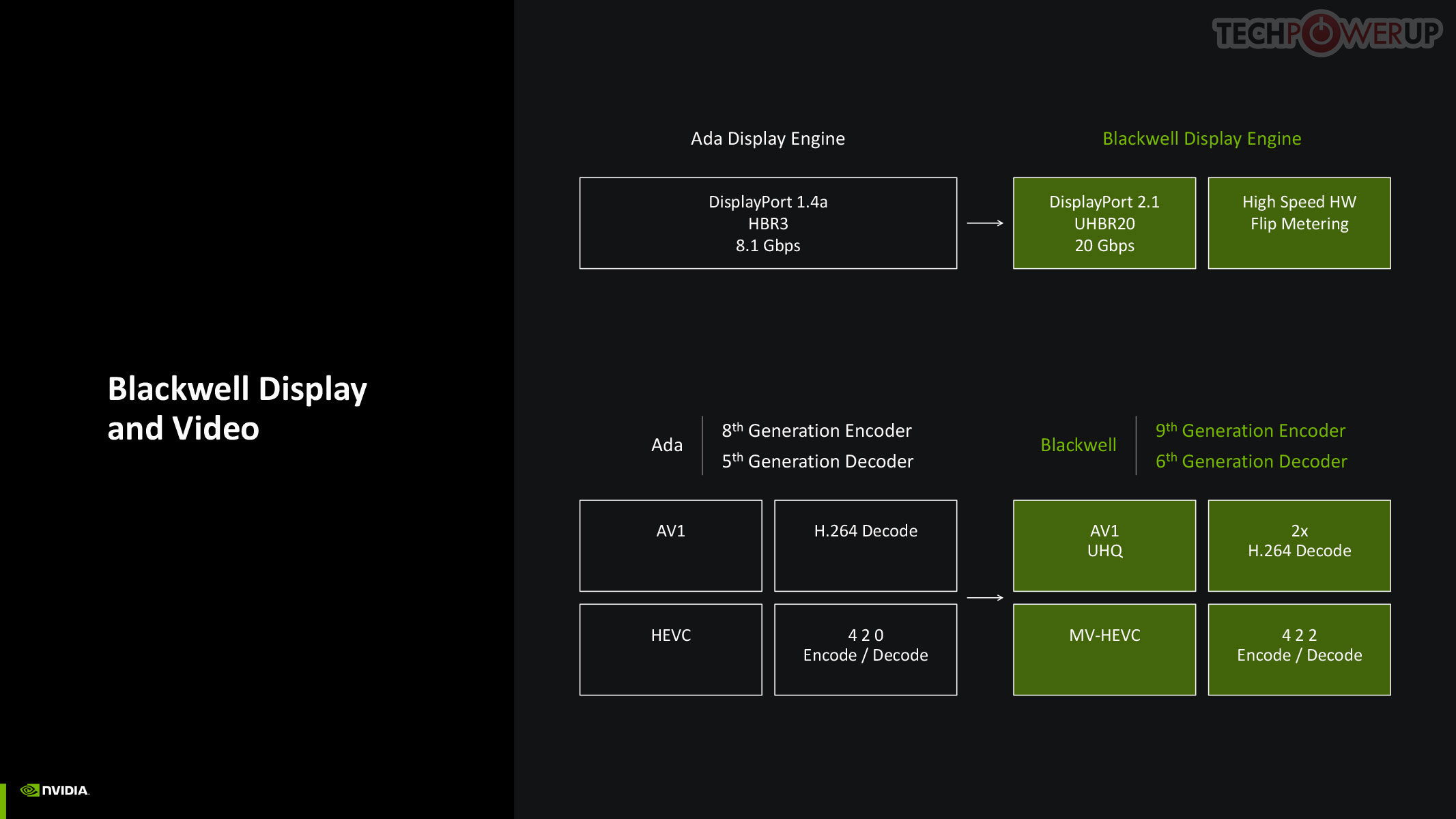
NVIDIA updated both the display engine and the media engine of Blackwell over the previous generation Ada, which drew some flack for holding on to older display I/O standards such as DisplayPort 1.4, while AMD and Intel had moved on to DisplayPort 2.1. The good news is that Blackwell supports DP 2.1 with UHBR20, enabling 8K 60 Hz with a single cable. The company also updated NVDEC and NVENC, which now support AV1 UHQ, double the H.264 decode performance, MV-HEVC, and 4:2:2 formats.
Jul 12th, 2025 00:53 CDT
change timezone
Latest GPU Drivers
New Forum Posts
- Can you guess Which game it is? (222)
- 'NVIDIA App' not usable offline? (7)
- What are you playing? (23920)
- RX 9070 XT freezing/locking up only on desktop, anyone else? (43)
- NVIDIA RTX PRO 6000 Workstation Runs Much Hotter Than 5090 FE (22)
- Quick charging your USB devicesUSB 3.2 Gen 2x2 Type-C® front-panel. (1)
- GTX 1050 GPU Owners Club (12)
- ASUS ProArt GeForce RTX 4060 Ti OC Edition 16GB GDDR6 Gaming - nvflash64 VBIOS mismatch (2)
- Will you buy a RTX 5090? (640)
- No offense, here are some things that bother me about your understanding of fans. (33)
Popular Reviews
- Fractal Design Epoch RGB TG Review
- Corsair FRAME 5000D RS Review
- Lexar NM1090 Pro 4 TB Review
- NVIDIA GeForce RTX 5050 8 GB Review
- NZXT N9 X870E Review
- Sapphire Radeon RX 9060 XT Pulse OC 16 GB Review - An Excellent Choice
- AMD Ryzen 7 9800X3D Review - The Best Gaming Processor
- Upcoming Hardware Launches 2025 (Updated May 2025)
- Our Visit to the Hunter Super Computer
- Chieftec Iceberg 360 Review
TPU on YouTube
Controversial News Posts
- Intel's Core Ultra 7 265K and 265KF CPUs Dip Below $250 (288)
- Some Intel Nova Lake CPUs Rumored to Challenge AMD's 3D V-Cache in Desktop Gaming (140)
- AMD Radeon RX 9070 XT Gains 9% Performance at 1440p with Latest Driver, Beats RTX 5070 Ti (131)
- NVIDIA Launches GeForce RTX 5050 for Desktops and Laptops, Starts at $249 (119)
- NVIDIA GeForce RTX 5080 SUPER Could Feature 24 GB Memory, Increased Power Limits (115)
- Microsoft Partners with AMD for Next-gen Xbox Hardware (105)
- Intel "Nova Lake‑S" Series: Seven SKUs, Up to 52 Cores and 150 W TDP (100)
- NVIDIA DLSS Transformer Cuts VRAM Usage by 20% (97)