 8
8
Palit GeForce RTX 4090 GameRock OC Review
Test Setup »High-resolution PCB Pictures
These pictures are for the convenience of volt modders and people who would like to see all the finer details on the PCB. Feel free to link back to us and use these in your articles, videos or forum posts.

High-resolution versions are also available (front, back).
Circuit Board (PCB) Analysis
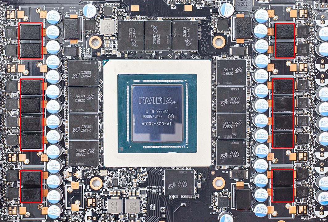
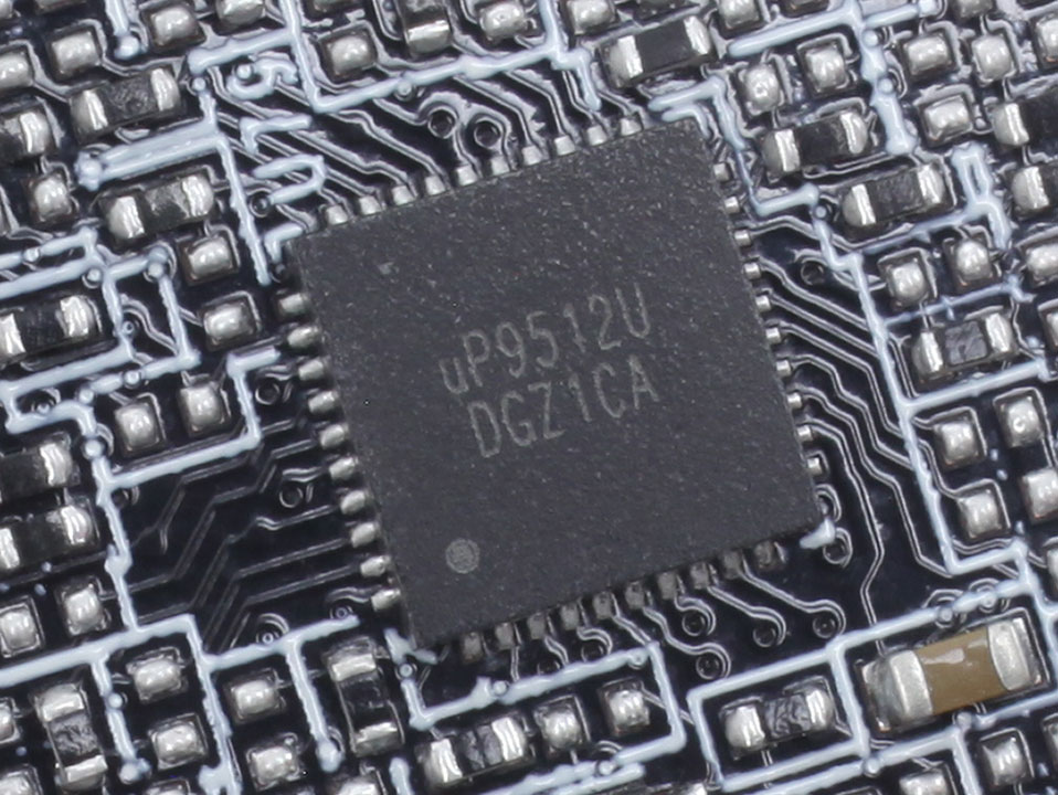
GPU voltage is a 16-phase design managed by a uPI uP9512U controller.
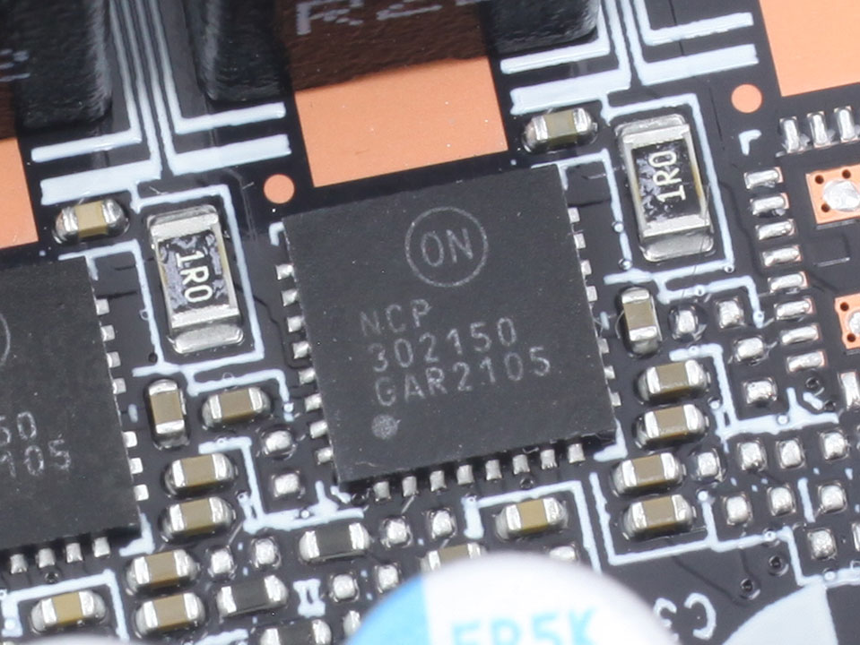
OnSemi NCP302150 DrMOS components are used for GPU voltage; they are rated for 50 A of current each.
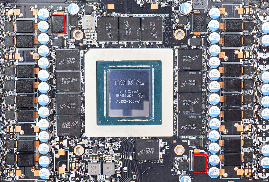
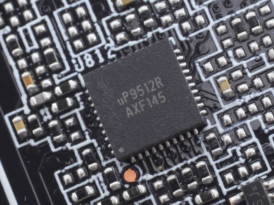
Memory voltage is a three-phase design, managed by a UPI uP9512R controller.
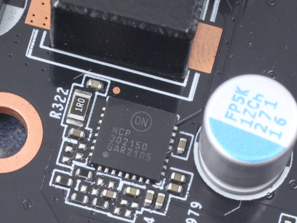
For memory, OnSemi NCP302150 DrMOS with a 50 A rating are used, too.
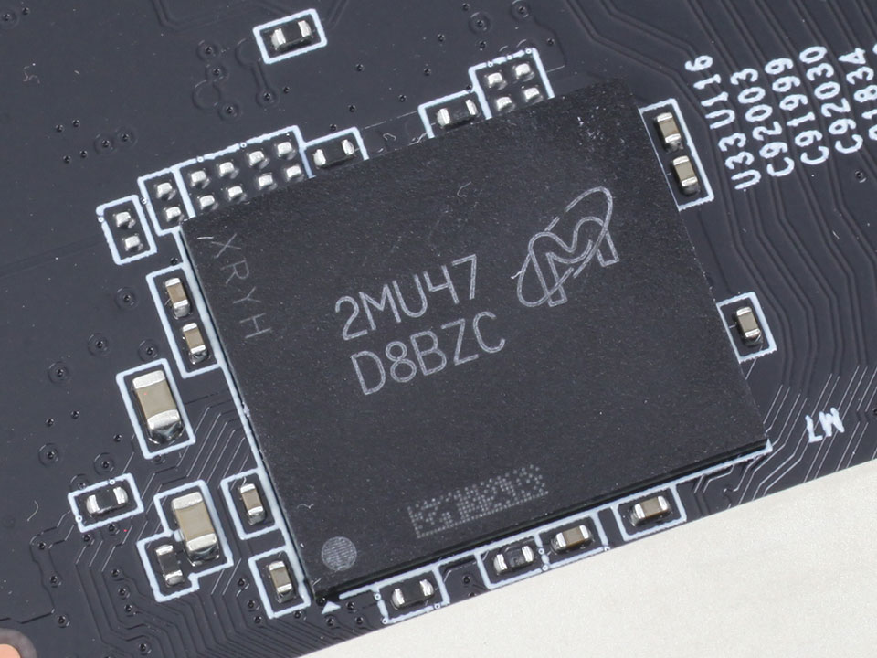
The GDDR6X memory chips are made by Micron and carry the model number D8BZC, which decodes to MT61K512M32KPA-21:U. They are specified to run at 1313 MHz (21 Gbps effective).
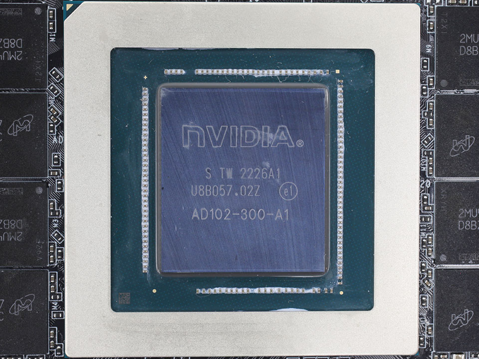
NVIDIA's AD102 graphics processor is the company's flagship Ada Lovelace GPU. It's the world's first 5 nanometer GPU, built at TSMC Taiwan with a transistor count of 76.3 billion and a die size of 608 mm².
Apr 2nd, 2025 03:03 EDT
change timezone
Latest GPU Drivers
New Forum Posts
- Help me pick a UPS (17)
- Which version of GPU-Z for Windows XP Pro 32 bit? (5)
- Free Games Thread (4606)
- Packing Ties vs. Cable/Zip Ties (6)
- Is RX 9070 VRAM temperature regular value or hotspot? (285)
- Is the futureproof gaming solution a four drive system? (45)
- Biostar RX 6700 XT OC BIOS (20)
- can i yust connect 4 pin cpu coler to 5 pin ? (13)
- Whats the Deal with the 570 nvidia drivers ? (8)
- Microprose: Falcon 5.0 - Well under development- yeay (6)
Popular Reviews
- DDR5 CUDIMM Explained & Benched - The New Memory Standard
- Sapphire Radeon RX 9070 XT Pulse Review
- SilverStone Lucid 04 Review
- ASRock Phantom Gaming B850 Riptide Wi-Fi Review - Amazing Price/Performance
- Palit GeForce RTX 5070 GamingPro OC Review
- Gigabyte GeForce RTX 5080 Gaming OC Review
- Sapphire Radeon RX 9070 XT Nitro+ Review - Beating NVIDIA
- Samsung 9100 Pro 2 TB Review - The Best Gen 5 SSD
- Assassin's Creed Shadows Performance Benchmark Review - 30 GPUs Compared
- be quiet! Pure Rock Pro 3 Black Review
Controversial News Posts
- MSI Doesn't Plan Radeon RX 9000 Series GPUs, Skips AMD RDNA 4 Generation Entirely (146)
- Microsoft Introduces Copilot for Gaming (124)
- AMD Radeon RX 9070 XT Reportedly Outperforms RTX 5080 Through Undervolting (119)
- NVIDIA Reportedly Prepares GeForce RTX 5060 and RTX 5060 Ti Unveil Tomorrow (115)
- Over 200,000 Sold Radeon RX 9070 and RX 9070 XT GPUs? AMD Says No Number was Given (100)
- NVIDIA GeForce RTX 5050, RTX 5060, and RTX 5060 Ti Specifications Leak (96)
- Retailers Anticipate Increased Radeon RX 9070 Series Prices, After Initial Shipments of "MSRP" Models (90)
- China Develops Domestic EUV Tool, ASML Monopoly in Trouble (88)