News Posts matching #5 nm

Return to Keyword Browsing

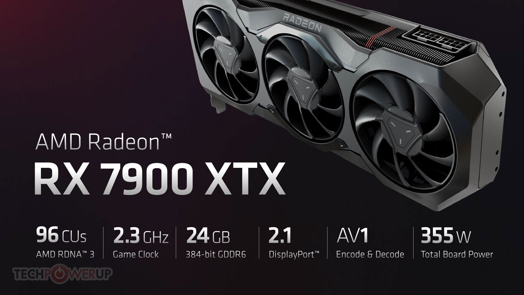
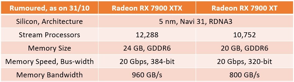
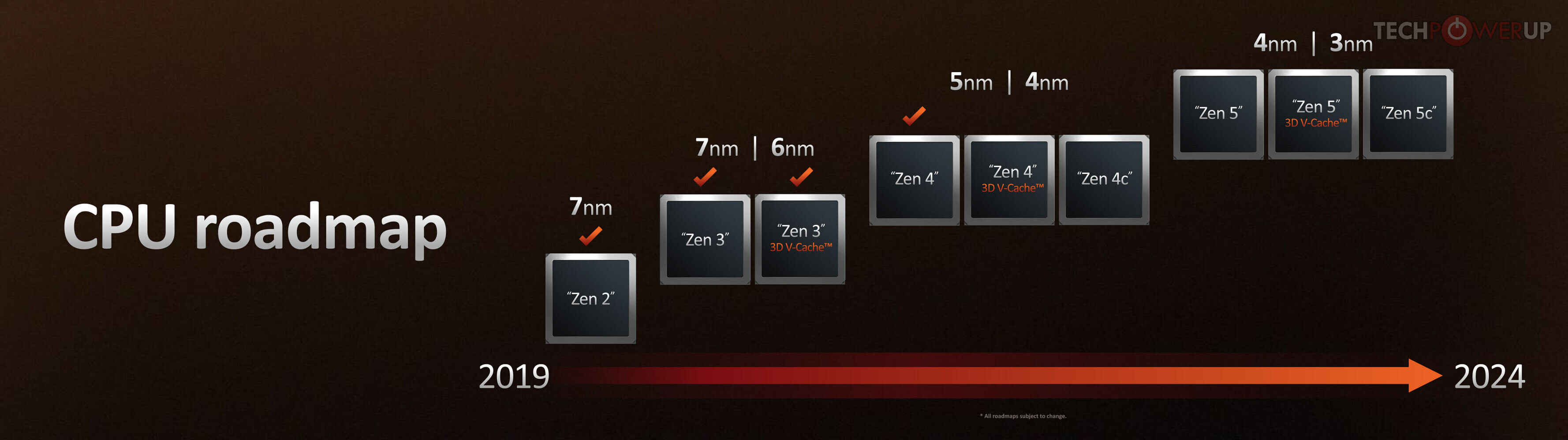
Huawei Prepares EUV Scanner for Sub-7 nm Chinese Chips

Huawei, the Chinese technology giant, has reportedly filed patents that it is developing extreme ultraviolet (EUV) scanners for use in the manufacturing process of semiconductors. This news comes amid increasing tensions between Huawei and the US government, which has imposed a series of sanctions on the company in recent years. According to UDN, Huawei has filed a patent that covers the entire EUV scanner with a 13.5 nm EUV light source, mirrors, lithography for printing circuits, and proper system control. While filing a patent is not the same as creating an accurate EUV scanner, it could enable China to produce a class of chips below 7 nm and have a homegrown semiconductor production, despite the ever-increasing US sanctions.

The development of EUV scanners is a significant milestone for Huawei and the semiconductor industry. However, the company's progress in this area may be hindered by the US government's sanctions, which have limited Huawei's access to certain technologies and markets. It is important to note that Chinese SMIC wanted to develop EUV fabrication based on third-party EUV tools; however, those plans were scrapped as the Wassenaar agreement came into action and prohibited the sales of advanced tools to Chinese companies. Huawei's development could represent a new milestone for the entire Chinese industry.

Global Top 10 Foundries' Total Revenue Grew by 6% QoQ for 3Q22, but Foundry Industry's Revenue Performance Will Enter Correction Period in 4Q22

According to TrendForce's research, the total revenue of the global top 10 foundries rose by 6% QoQ to US$35.21 billion for 3Q22 as the release of the new iPhone series during the second half of the year generated significant stock-up activities across Apple's supply chain. However, the global economy shows weak performances, and factors such as China's policy on containing COVID-19 outbreaks and high inflation continue to impact consumer confidence. As a result, peak-season demand in the second half of the year has been underwhelming, and inventory consumption is proceeding slower than anticipated. This situation has led to substantial downward corrections to foundry orders as well. For 4Q22, TrendForce forecasts that the total revenue of the global top 10 foundries will register a QoQ decline, thereby terminating the boom of the past two years—when there was an uninterrupted trend of QoQ revenue growth.

Regarding individual foundries' performances in 3Q22, the group of the top five was led by TSMC, followed by Samsung, UMC, GlobalFoundries, and SMIC. Their collective global market share (in revenue terms) came to 89.6%. Most foundries were directly impacted by clients slowing down their stock-up activities or significantly correcting down their orders. Only TSMC was able to make a notable gain due to Apple's strong stock-up demand for the SoCs deployed in this year's new iPhone models. TSMC saw its revenue rise by 11.1% QoQ to US$20.16 billion, and the corresponding market share expanded to 56.1%. The growth was mainly attributed to the ≤7 nm nodes, whose share in the foundry's revenue had kept climbing and reached 54% in the third quarter. Conversely, Samsung actually experienced a slight QoQ drop of 0.1% in foundry revenue even though it had also benefited from the component demand related to the new iPhone series. Partially impacted by the weakening of the Korean won, Samsung's market share fell to 15.5%.

Apple and NVIDIA First Customers of TSMC's Arizona Fab

Apple and NVIDIA will be among the first customers of TSMC's swanky new $12 billion semiconductor fab in Arizona, USA. Apple will be the first major player to kick off mass-production in the fab, and will be closely followed by NVIDIA. Both companies plan to produce some of their inventory in Arizona, and ramp proportionately up as the fab grows in capacity.

The plan with TSMC's Arizona fab was to originally make 5 nm and 4 nm EUV chips, with an output of 20,000 wafers a month, but the company now expects to deploy a more advanced node to keep up with what will be considered cutting-edge when the fab goes live (think 2 nm-class); and also double the output to 40,000 wafers a month. The capacity should ensure Apple and NVIDIA make their most cutting-edge chips on the node (away from Asia), so there could be tighter export controls, and build supply-chain resilience in the face of security problems arising in the Taiwan straits.

AMD RDNA3 Second-largest Navi 32 and Third-largest Navi 33 Shader Counts Leaked

The unified shader (stream processor) counts of AMD's upcoming second- and third-largest GPUs based on the RDNA3 graphics architecture, have been leaked in some ROCm code, discovered by Kepler_L2 on Twitter. The "performance.hpp" file references "Navi 32" with a compute unit count of 60, and the "Navi 33" with 32 compute units. We know from the "Navi 31" specifications that an RDNA3 compute unit still amounts to 64 stream processors (although with significant IPC uplifts over the RDNA2 stream processor due to dual-instruction issue-rate).

60 compute units would give the "Navi 32" silicon a stream processor count of 3,840, a 50% numerical increase over the 2,560 of its predecessor, the "Navi 22," powering graphics cards such as the Radeon RX 6750 XT. Meanwhile, the 32 CU count of the "Navi 33" amounts to 2,048 stream processors, which is numerically unchanged from that of the "Navi 23" powering the RX 6650 XT. The new RDNA3 compute unit has significant changes over RDNA2, besides the dual-issue stream processors—it gets second-generation Ray Accelerators, and two AI accelerators for matrix-multiplication.

TSMC 3 nm Wafer Pricing to Reach $20,000; Next-Gen CPUs/GPUs to be More Expensive

Semiconductor manufacturing is a significant investment that requires long lead times and constant improvement. According to the latest DigiTimes report, the pricing of a 3 nm wafer is expected to reach $20,000, which is a 25% increase in price over a 5 nm wafer. For 7 nm, TSMC managed to produce it for "just" $10,000; for 5 nm, it costs the company to make it for the $16,000 mark. And finally, the latest and greatest technology will get an even higher price point at $20,000, a new record in wafer pricing. Since TSMC has a proven track record of delivering constant innovation, clients are expected to remain on the latest tech purchasing spree.

Companies like Apple, AMD, and NVIDIA are known for securing orders for the latest semiconductor manufacturing node capacities. With a 25% increase in wafer pricing, we can expect the next-generation hardware to be even more expensive. Chip manufacturing price is a significant price-determining factor for many products, so the 3 nm edition of CPUs, GPUs, etc., will get the highest difference.

TSMC's Morris Chang Says Arizona Fab Will Produce 3 nm Chips in the Future

Although Morris Chang is no longer in charge of the day to day business at TSMC, the founder of the company is still getting his hands dirty. Chang attended the APEC Economic Leaders Meeting last week, as part of Taiwan's delegation and was questioned by the media about TSMC's future plans. The specific question was about TSMC's Arizona fab, which will initially produce chips using a 5 nm node. The US$12 billion plant is scheduled to kick off production at some point in 2024, by which time the 5 nm node should be a commonly used node rather than close to cutting edge.

When questioned about the future of the Arizona fab, Morris Chang answered that it will be moving to a 3 nm node, which is currently TSMC's most cutting edge node, that has gone into volume production earlier this year with th N3 node, which is set to be followed by the N3E node. According to Chang, there's interest by several countries to have TSMC set up fabs there, but apparently this is not something TSMC is considering at the moment. One potential reason for this would be a suitable labour force, something that has already proven to be tough for the Arizona fab.

AMD Explains the Economics Behind Chiplets for GPUs

AMD, in its technical presentation for the new Radeon RX 7900 series "Navi 31" GPU, gave us an elaborate explanation on why it had to take the chiplets route for high-end GPUs, devices that are far more complex than CPUs. The company also enlightened us on what sets chiplet-based packages apart from classic multi-chip modules (MCMs). An MCM is a package that consists of multiple independent devices sharing a fiberglass substrate.

An example of an MCM would be a mobile Intel Core processor, in which the CPU die and the PCH die share a substrate. Here, the CPU and the PCH are independent pieces of silicon that can otherwise exist on their own packages (as they do on the desktop platform), but have been paired together on a single substrate to minimize PCB footprint, which is precious on a mobile platform. A chiplet-based device is one where a substrate is made up of multiple dies that cannot otherwise independently exist on their own packages without an impact on inter-die bandwidth or latency. They are essentially what should have been components on a monolithic die, but disintegrated into separate dies built on different semiconductor foundry nodes, with a purely cost-driven motive.

Eliyan Closes $40M Series A Funding Round and Unveils Industry's Highest Performance Chiplet Interconnect Technologies

Eliyan Corporation, credited for the invention of the semiconductor industry's highest-performance and most efficient chiplet interconnect, today announced two major milestones in the commercialization of its technology for multi-die chiplet integration: the close of its Series A $40M funding round, and the successful tapeout of its technology on an industry standard 5-nanometer (nm) process.

Eliyan's NuLink PHY and NuGear technologies address the critical need for a commercially viable approach to enabling high performance and cost-effectiveness in the connection of homogeneous and heterogenous architectures on a standard, organic chip substrate. It has proven to achieve similar bandwidth, power efficiency, and latency as die-to-die implementations using advanced packaging technologies, but without the other drawbacks of specialized approaches.

AMD RDNA3 Navi 31 GPU Block Diagram Leaked, Confirmed to be PCIe Gen 4

An alleged leaked company slide details AMD's upcoming 5 nm "Navi 31" GPU powering the next-generation Radeon RX 7900 XTX and RX 7900 XT graphics cards. The slide details the "Navi 31" MCM, with its central graphics compute die (GCD) chiplet that's built on the 5 nm EUV silicon fabrication process, surrounded by six memory cache dies (MCDs), each built on the 6 nm process. The GCD interfaces with the system over a PCI-Express 4.0 x16 host interface. It features the latest-generation multimedia engine with dual-stream encoders; and the new Radiance display engine with DisplayPort 2.1 and HDMI 2.1a support. Custom interconnects tie it with the six MCDs.

Each MCD has 16 MB of Infinity Cache (L3 cache); and a 64-bit GDDR6 memory interface (two 32-bit GDDR6 paths). Six of these add up to the GPU's 384-bit GDDR6 memory interface. In the scheme of things, the GPU has a contiguous and monolithic 384-bit wide memory bus, because every modern GPU uses multiple on-die memory controllers to achieve a wide memory bus. "Navi 31" hence has a total Infinity Cache size of 96 MB—which may be less in comparison to the 128 MB on "Navi 21," but AMD has shored up cache sizes across the GPU. The L0 caches on the compute units is now increased numerically by 240%. The L1 caches by 300%, and the L2 cache shared among the shader engines, by 50%. The RX 7900 XTX is confirmed to use 20 Gbps GDDR6 memory in this slide, for 960 GB/s of memory bandwidth.

AMD Announces the $999 Radeon RX 7900 XTX and $899 RX 7900 XT, 5nm RDNA3, DisplayPort 2.1, FSR 3.0 FluidMotion

AMD today announced the Radeon RX 7900 XTX and Radeon RX 7900 XT gaming graphics cards debuting its next-generation RDNA3 graphics architecture. The two new cards come at $999 and $899—basically targeting the $1000 high-end premium price point.
Both cards will be available on December 13th, not only the AMD reference design, which is sold through AMD.com, but also custom-design variants from the many board partners on the same day. AIBs are expected to announce their products in the coming weeks.

The RX 7900 XTX is priced at USD $999, and the RX 7900 XT is $899, which is a surprisingly small difference of only $100, for a performance difference that will certainly be larger, probably in the 20% range. Both Radeon RX 7900 XTX and RX 7900 XT are using the PCI-Express 4.0 interface, Gen 5 is not supported with this generation. The RX 7900 XTX has a typical board power of 355 W, or about 95 W less than that of the GeForce RTX 4090. The reference-design RX 7900 XTX uses conventional 8-pin PCIe power connectors, as would custom-design cards, when they come out. AMD's board partners will create units with three 8-pin power connectors, for higher out of the box performance and better OC potential. The decision to not use the 16-pin power connector that NVIDIA uses was made "well over a year ago", mostly because of cost, complexity and the fact that these Radeons don't require that much power anyway.

AMD Navi 31 RDNA3 GPU Pictured

Here's the first picture of the "Navi 31" GPU at the heart of AMD's fastest next-generation graphics cards. Based on the RDNA3 graphics architecture, this will mark an ambitious attempt by AMD to build the first multi-chip module (MCM) client GPU featuring more than one logic die. MCM GPUs aren't new in the enterprise space with Intel's "Ponte Vecchio," but this would be the first such GPU meant for hardcore gaming graphics products. AMD had made MCM GPUs in the past, but those have been packages with just one logic die, surrounded by memory stacks. "Navi 31" is an MCM of as many as eight logic dies, and no memory stacks (no, those aren't HBM stacks in the picture below).

It's rumored that "Navi 31" features one or two SIMD chiplets dubbed GCDs, featuring the GPU's main number crunching machinery, the RDNA3 compute units. These chiplets are likely built on the most advanced silicon fabrication node, likely TSMC 5 nm EUV, but we'll see. The GDDR6 memory controllers handling the chip's 384-bit wide GDDR6 memory interface, will be located on separate chiplets built on a slightly older node, such as TSMC 6 nm. This is not multi-GPU-a-stick, because both SIMD chiplets have uniform access to the entire 384-bit wide memory bus (which is not 2x 192-bit but 1x 384-bit), besides the other ancillaries. The "Navi 31" MCM are expected to be surrounded by JEDEC-standard 20 Gbps GDDR6 memory chips.

AMD Reports Third Quarter 2022 Financial Results

AMD (NASDAQ:AMD) today announced revenue for the third quarter of 2022 of $5.6 billion, gross margin of 42%, operating loss of $64 million, net income of $66 million and diluted earnings per share of $0.04. On a non-GAAP(*) basis, gross margin was 50%, operating income was $1.3 billion, net income was $1.1 billion and diluted earnings per share was $0.67.

"Third quarter results came in below our expectations due to the softening PC market and substantial inventory reduction actions across the PC supply chain," said AMD Chair and CEO Dr. Lisa Su. "Despite the challenging macro environment, we grew revenue 29% year-over-year driven by increased sales of our data center, embedded and game console products. We are confident that our leadership product portfolio, strong balance sheet, and ongoing growth opportunities in our data center and embedded businesses position us well to navigate the current market dynamics."

SiFive's New High-Performance Processors Offer a Significant Upgrade for Wearable and Consumer Products

SiFive, Inc. the founder and leader of RISC-V computing, today announced two new products that address the need for high performance and efficiency in a small size in high volume applications like wearables, smart home, industrial automation, AR/VR, and other consumer devices. The SiFive Performance P670 and P470 RISC-V processors bring unparalleled compute performance and efficiency that is significantly raising the bar for innovative designs in these high-volume markets. The modern and innovative SiFive design methodologies bring raw compute density that is a substantial advantage for SiFive Performance products and also translates into significant cost savings for customers.

"The P670 and P470 are specifically designed for, and capable of handling the most demanding workloads for wearables and other advanced consumer applications. These new products offer powerful performance and compute density for companies looking to upgrade from legacy ISAs," said Chris Jones, SiFive VP of Product. "We have optimized these new RISC-V Vector enabled products to deliver the performance and efficiency improvements the industry has long been asking for, and we are in evaluations with a number of top-tier customers. Additionally, as the upstream enablement of RISC-V has started within the Android Open Source Project, (AOSP), designers will have unrivaled choice and flexibility as they consider the positive implications with that platform for future designs."

AMD Radeon RX 7000 RDNA3 To Launch Early December

AMD's next-generation Radeon RX 7000-series graphics cards based on the RDNA3 graphics architecture, are expected to launch in early-December 2022, according to greymon55, a reliable source with AMD leaks. The cards will be unveiled at a media event to be held on November 3, 2022, with market availability following a month after (between 1st to 5th December). The company is expected to take a top-down product-stack release cycle similar to that of NVIDIA, with the release of two of its top SKUs, the Radeon RX 7900 XTX and the RX 7900 XT. Both these cards are based on the 5 nm Navi 31 MCM GPU. This will be AMD's first client-graphics MCM GPU with more than one logic die. The company has a decade of experience with MCMs, but past generations have been one logic die surrounded with on-package HBM. Navi 31 has on-package logic chiplets, but discrete GDDR6 memory, like most other GPUs in the market today. It's rumored that the company is targeting a 100% performance uplift over the previous-generation, which means team-red is on the prowl to compete with NVIDIA's fastest SKUs, including the RTX 4090 and upcoming RTX 4080.

Intel's Next-Gen Desktop Platform Intros Socket LGA1851, "Meteor Lake-S" to Feature 6P+16E Core Counts

Keeping up with the cadence of two generations of desktop processors per socket, Intel will turn the page of the current LGA1700, with the introduction of the new Socket LGA1851. The processor package will likely have the same dimensions as LGA1700, and the two sockets may share cooler compatibility. The first processor microarchitecture to debut on LGA1851 will be the 14th Gen Core "Meteor Lake-S." These chips will feature a generationally lower CPU core-count compared to "Raptor Lake," but significantly bump the IPC on both the P-cores and E-cores.

"Raptor Lake" is Intel's final monolithic silicon client processor before the company pivots to chiplets built on various foundry nodes, as part of its IDM 2.0 strategy. The client-desktop version of "Meteor Lake," dubbed "Meteor Lake-S," will have a maximum CPU core configuration of 6P+16E (that's 6 performance cores with 16 efficiency cores). The chip has 6 "Redwood Cove" P-cores, and 16 "Crestmont" E-cores. Both of these are expected to receive IPC uplifts, such that the processor will end up faster (and hopefully more efficient) than the top "Raptor Lake-S" part. Particularly, it should be able to overcome the deficit of 2 P-cores.

IBM Artificial Intelligence Unit (AIU) Arrives with 23 Billion Transistors

IBM Research has published information about the company's latest development of processors for accelerating Artificial Intelligence (AI). The latest IBM processor, called the Artificial Intelligence Unit (AIU), embraces the problem of creating an enterprise solution for AI deployment that fits in a PCIe slot. The IBM AIU is a half-height PCIe card with a processor powered by 23 Billion transistors manufactured on a 5 nm node (assuming TSMC's). While IBM has not provided many details initially, we know that the AIU uses an AI processor found in the Telum chip, a core of the IBM Z16 mainframe. The AIU uses Telum's AI engine and scales it up to 32 cores and achieve high efficiency.

The company has highlighted two main paths for enterprise AI adoption. The first one is to embrace lower precision and use approximate computing to drop from 32-bit formats to some odd-bit structures that hold a quarter as much precision and still deliver similar result. The other one is, as IBM touts, that "AI chip should be laid out to streamline AI workflows. Because most AI calculations involve matrix and vector multiplication, our chip architecture features a simpler layout than a multi-purpose CPU. The IBM AIU has also been designed to send data directly from one compute engine to the next, creating enormous energy savings."

TSMC Cuts Back CAPEX Budget Despite Record Profits

Another quarter, another record breaking earnings report by TSMC, but it seems like the company has released that things are set to slow down sooner than initially expected and the company is hitting the brakes on some of its expansion projects. The company saw a 79.7 percent increase in profits compared to last year, with a profit of US$8.8 billion and a revenue of somewhere between US$19.9 to US$ 20.7 billion for the third quarter, which is a 47.9 percent bump compared to last year. TSMC's 5 nm nodes were the source for 28 percent of the revenues, followed by 26 percent for 7 nm nodes, 12 percent for 16 nm and 10 percent for 28 nm, with remaining nodes at 40 nm and larger making up for the remainder of the revenue. By platform, smartphone chips made up 41 percent, followed by High Performance Computing at 39 percent, IoT at 10 percent and automotive at five percent.

TSMC said it will cut back its CAPEX budget by around US$4 billion, to US$36 billion, compared to the earlier stated US$40 billion budget the company had set aside for expanding its fabs. Part of the reason for this is that TSMC is already seeing weaker demand for products manufactured using its N7 and N6 nodes, as the N7 node was meant to be a key part of the new fab in Kaohsiung in southern Taiwan. TSMC is expecting to start production on its first N3 node later this quarter and is expecting the capacity to be fully utilised for all of 2023. Supply is said to be exceeding demand, which TSMC said is partially to blame on tooling delivery issues. TSMC is expecting next year's revenue for its N3 node to be higher than its N5 node in 2020, although the revenue is said to be in the single digit percentage range. The N3E node is said to start production sometime in the second half of next year, or about a quarter earlier than expected. The N2 node isn't due to start production until 2025, but TSMC is already having very high customer engagement, so it doesn't look like TSMC is likely to suffer from a lack of business in the foreseeable future, as long as the company keeps delivering new nodes as planned.

AMD RDNA3 Radeon RX 7000 Flagship GPU PCB Sketched

Here's the very first sketch of an AMD RDNA3 Radeon RX 7000-series flagship graphics card with the "Navi 31" chip in the middle. This will be AMD's first chiplet-based GPU built on a philosophy similar to that of the Ryzen desktop and EPYC server processors. The main number crunching machinery that benefits the most from the latest foundry process, will be built on 5 nm logic chiplets (up to two of these on the "Navi 31," one of these on the "Navi 32"), while the components that don't really benefit from the latest process, such as the memory controllers, display/media accelerators, etc., will be disintegrated into chiplets built on a slightly older node, such as 6 nm. This way AMD gets to maximize its 5 nm allocation at TSMC, which it has to share among not just the logic tiles of RDNA3 GPUs, but also its "Zen 4" processors.

The top-dog "Navi 31" silicon is expected to feature a 384-bit wide GDDR6 memory interface, which is why you see 12 memory chips surrounding the GPU package. AMD is expected to deploy fast 19-21 Gbps class GDDR6 memory chips, as well as double-down on the Infinity Cache technology. The package looks like a GPU die surrounded by HBM stacks, but those are actually the memory/display chiplets. If this PCB is from an AMD reference design, it could be the biggest hint that AMD isn't switching over to the 12+4 pin ATX 12HPWR connector just yet, and could stick with three 8-pin PCIe connectors for power, just like the current RX 6950 XT. USB-C with DisplayPort passthrough could prominently feature with RDNA3 graphics cards, besides standard DisplayPort and HDMI connectors.

NVIDIA AD102 "Ada" Packs Over 75 Billion Transistors

NVIDIA's next-generation AD102 "Ada" GPU is shaping up to be a monstrosity, with a rumored transistor-count north of 75 billion. This would put over 2.6 times the 28.3 billion transistors of the current-gen GA102 silicon. NVIDIA is reportedly building the AD102 on the TSMC N5 (5 nm EUV) node, which offers a significant transistor-density uplift over the Samsung 8LPP (8 nm DUV) node on which the GA102 is built. The 8LPP offers 44.56 million transistors per mm² die-area (MTr/mm²), while the N5 offers a whopping 134 MTr/mm², which fits in with the transistor-count gain. This would put its die-area in the neighborhood of 560 mm². The AD102 is expected to power high-end RTX 40-series SKUs in the RTX 4090-series and RTX 4080-series.

AMD EPYC "Genoa" Zen 4 Product Stack Leaked

With its recent announcement of the Ryzen 7000 desktop processors, the action now shifts to the server, with AMD preparing a wide launch of its EPYC "Genoa" and "Bergamo" processors this year. Powered by the "Zen 4" microarchitecture, and contemporary I/O that includes PCI-Express Gen 5, CXL, and DDR5, these processors dial the CPU core-counts per socket up to 96 in case of "Genoa," and up to 128 in case of "Bergamo." The EPYC "Genoa" series represents the main trunk of the company's server processor lineup, with various internal configurations targeting specific use-cases.

The 96 cores are spread twelve 5 nm 8-core CCDs, each with a high-bandwidth Infinity Fabric path to the sIOD (server I/O die), which is very likely built on the 6 nm node. Lower core-count models can be built either by lowering the CCD count (ensuring more cores/CCD), or by reducing the number of cores/CCD and keeping the CCD-count constant, to yield more bandwidth/core. The leaked product-stack table below shows several of these sub-classes of "Genoa" and "Bergamo," classified by use-cases. The leaked slide also details the nomenclature AMD is using with its new processors. The leaked roadmap also mentions the upcoming "Genoa-X" processor for HPC and cloud-compute uses, which features the 3D Vertical Cache technology.

AMD "Zen 4" Dies, Transistor-Counts, Cache Sizes and Latencies Detailed

As we await technical documents from AMD detailing its new "Zen 4" microarchitecture, particularly the all-important CPU core Front-End and Branch Prediction units that have contributed two-thirds of the 13% IPC gain over the previous-generation "Zen 3" core, the tech enthusiast community is already decoding images from the Ryzen 7000 series launch presentation. "Skyjuice" presented the first annotation of the "Zen 4" core, revealing its large branch-prediction unit, enlarged micro-op cache, TLB, load/store unit, and dual-pumped 256-bit FPU that enables AVX-512 support. A quarter of the core's die-area is also taken up by the 1 MB dedicated L2 cache.

Chiakokhua (aka Retired Engineer) posted a table detailing the various caches and their latencies, comparing it with those of the "Zen 3" core. As AMD's Mark Papermaster revealed in the Ryzen 7000 launch event, the company has enlarged the micro-op cache of the core from 4 K entries to 6.75 K entries. The L1I and L1D caches remain 32 KB in size, each; while the L2 cache has doubled in size. The enlargement of the L2 cache has slightly increased latency, from 12 cycles to 14. Latency of the shared L3 cache is also up, from 46 cycles to 50 cycles. The reorder buffer (ROB) in the dispatch stage has been enlarged from 256 entries to 320 entries. The L1 branch target buffer (BTB) has increased in size from 1 KB to 1.5 KB.

AMD Confirms Optical-Shrink of Zen 4 to the 4nm Node in its Latest Roadmap

AMD in its Ryzen 7000 series launch event shared its near-future CPU architecture roadmap, in which it confirmed that the "Zen 4" microarchitecture, currently on the 5 nm foundry node, will see an optical-shrink to the 4 nm process in the near future. This doesn't necessarily indicate a new-generation CCD (CPU complex die) on 4 nm, it could even be a monolithic mobile SoC on 4 nm, or perhaps even "Zen 4c" (high core-count, low clock-speed, for cloud-compute); but it doesn't rule out the possibility of a 4 nm CCD that the company can use across both its enterprise and client processors.

The last time AMD hyphenated two foundry nodes for a single generation of the "Zen" architecture, was with the original (first-generation) "Zen," which debuted on the 14 nm node, but was optically shrunk and refined on the 12 nm node, with the company designating the evolution as "Zen+." The Ryzen 7000-series desktop processors, as well as the upcoming EPYC "Genoa" server processors, will ship with 5 nm CCDs, with AMD ticking it off in its roadmap. Chronologically placed next to it are "Zen 4" with 3D Vertical Cache (3DV Cache), and the "Zen 4c." The company is planning "Zen 4" with 3DV Cache both for its server- and desktop segments. Further down the roadmap, as we approach 2024, we see the company debut the future "Zen 5" architecture on the same 4 nm node, evolving into 3 nm on certain variants.

AMD Announces Ryzen 7000 Series "Zen 4" Desktop Processors

AMD today announced the Ryzen 7000 series "Zen 4" desktop processors. These debut the company's new "Zen 4" architecture to the market, increasing IPC, performance, with new-generation I/O such as DDR5 and PCI-Express Gen 5. AMD hasn't increased core-counts over the previous-generation, the Ryzen 5 series is still 6-core/12-thread, the Ryzen 7 8-core/16-thread, and Ryzen 9 either 12-core/24-thread, or 16-core/32-thread; but these are all P-cores. AMD is claiming a 13% IPC uplift generation over generation, which coupled with faster DDR5 memory, and CPU clock speeds of up to 5.70 GHz, give the Ryzen 7000-series processor an up to 29% single-core performance gain over the Ryzen 5000 "Zen 3."

At their press event, AMD showed us an up to 35% increase in gaming performance over the previous-generation, and an up to 45% increase in creator performance (which is where it gets the confidence to stick to its core-counts from). The "Zen 4" CPU core dies (CCDs) are built on the TSMC 5 nm EUV (N5) node. Even the I/O die sees a transition to 6 nm (N6), from 12 nm. The switch to 5 nm gives "Zen 4" 62 percent lower power for the same performance, or 49% more performance for the same power. versus the Ryzen 5000 series on 7 nm. The "Zen 4" core along with its dedicated L2 cache is 50% smaller, and 47% more energy efficient than the "Golden Cove" P-core of "Alder Lake."

AMD Ready with Zen 4 3DV Cache Chiplet, Expects to Repeat 5800X3D Magic Versus Raptor Lake

AMD is allegedly ready with a working "Zen 4" chiplet that has stacked 3D Vertical Cache (3DV cache) memory, which supplements the on-die L3 cache, and is found to massively improve gaming performance. "Moore's Law is Dead" reports that the Zen 4 + 3DV Cache chiplet will be used with various Ryzen 7000X3D SKUs, as well as special EPYC "Genoa" SKUs.

The 3DV Cache deployed with the "Zen 4" chiplet is a second-generation to the one on the "Zen 3 + 3DV cache" chiplet, and AMD has worked on a number of bandwidth and latency improvements, so it performs in-sync with the generationally-faster on-die L3 cache of the "Zen 4" chiplet. Unlike the CCD below it that's built on TSMC N5 (5 nm EUV), the L3D (the stacked die with the 3DV cache) is possibly be built on an older node, such as N6 (6 nm), since it only contains a slab of memory and doesn't warrant N5. "Moore's Law is Dead" reports that AMD expects to repeat the magic of the 5800X3D when it comes to gaming performance, and expects Ryzen 7000X3D processors to dominate Intel's 13th Gen "Raptor Lake" processors. This was echoed by another reliable source, greymon55.

AMD TSMC's Second Largest Customer for 5nm, More Resilient Than Intel to Face Downturns in the PC Industry: Report

AMD is now TSMC's second largest customer for its 5 nanometer N5 silicon fabrication node, according to a DigiTimes report. The Taiwan-based semiconductor industry observer also reports that AMD is more resilient than Intel in facing any downturns in the PC industry, in the coming few months. PC sales are expected to slump by as much as 15 percent in the near future, but the lower market-share compared to Intel; and the flexibility for AMD to move its CPU chips over to enterprise product to feed the growth in server processor segment, means that the company can ride over a bumpy road in the near future. The lower market-share translates to "lesser pain" from a slump compared to Intel. The report also says that embracing TSMC for processors "just in time" means that AMD has a front-row seat with product performance, time-to-market, yields, and delivery.

AMD is on the anvil of two major product launches on 5 nm, the Ryzen 7000 series "Raphael" desktop processors on August 30 (according to the report), and EPYC "Genoa" server processors in November 2022. The company is planning to refresh its notebook processor lineup in the first half of 2023, with "Dragon Range," and "Phoenix Point" targeting distinct market segments among notebooks. "Dragon Range" is essentially "Raphael" (5 nm chiplet + 6 nm cIOD) on a mobile-optimized BGA package, letting AMD cram up to 16 "Zen 4" cores, and take on Intel's high core-count mobile processors. The iGPU of "Dragon Range" will be basic, since designs based on this chip are expected to use discrete GPUs. "Phoenix Point" is a purpose-built mobile processor with up to 8 "Zen 4" cores, and a powerful iGPU based the RDNA3 architecture.
Return to Keyword Browsing
May 21st, 2024 11:50 EDT change timezone

New Forum Posts

Popular Reviews

Controversial News Posts