News Posts matching #5 nm

Return to Keyword Browsing

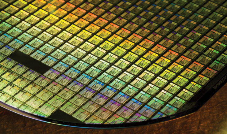
Marvell Announces Industry's First 112G 5nm SerDes Solution for Scaling Cloud Data Center Infrastructure

Marvell today unveiled the industry's first 112G 5 nm SerDes solution that has been validated in hardware. The DSP-based SerDes boasts industry-leading performance, power and area, helping to propel 112G as the interconnect of choice for next generation 5G, enterprise, and cloud data center infrastructure. Marvell has recently secured a new custom ASIC design win customer that will embed this new IP to build next generation top-of-rack (ToR) and spine switches for leading hyperscale data centers around the world. The Marvell 5 nm SerDes solution doubles the bandwidth of current systems based on 56G while enabling the deployment of 112G I/Os in many exciting new applications, including network and data center switching, network traffic management, machine learning training and inference, and application-specific accelerators.

Today's news, which comes on the heels of the company's announcement with TSMC of its 5 nm portfolio, further strengthens Marvell's leading data infrastructure offerings in the industry's most advanced process geometry. The 112G 5 nm SerDes solution is part of Marvell's industry-leading IP portfolio that addresses the full spectrum of infrastructure requirements and includes processor subsystems, encryption engines, system-on-chip fabrics, chip-to-chip interconnects, and a variety of physical layer interfaces.

Samsung Could Become Apple's Newest Chip Supplier

Apple has recently announced its transition to Apple Silicon, meaning that every processor inside its products will be custom designed by the company. However, that seems to be becoming a bit of a problem. The sole supplier of chips for Apple has been Taiwan Semiconductor Manufacturing Company (TSMC), which Apple collaborated with for the past few years. The sheer capacity of TSMC is enough to satisfy the demand from several companies and thus it allows some of them to book its capacity. With Apple demanding more and more capacity than ever before, it is becoming quite hard to keep up with it. That is why Apple is, according to some analysts for Business Korea, looking for a foundry beyond TSMC's to manufacture its chips.

According to the source, Apple is looking at the direction of Samsung Electronics and its silicon manufacturing facilities. Samsung has recently started the production of its 5 nm silicon manufacturing node. We have reported that the first SoCs are set to arrive soon. However, it may be possible that Apple's M1 lineup of SoCs will be a part of that first wave. Apple is reportedly going to tap both TSMC and Samsung to qualify enough supply for the huge demand of the products based on the latest 5 nm technology.

Samsung's 5 nm Node in Production, First SoCs to Arrive Soon

During its Q3 earnings call, Samsung Electronics has provided everyone with an update on its foundry and node production development. In the past year or so, Samsung's foundry has been a producer of a 7 nm LPP (Low Power Performance) node as its smallest node. That is now changed as Samsung has started the production of the 5 nm LPE (Low Power Early) semiconductor manufacturing node. In the past, we have reported that the company struggled with yields of its 5 nm process, however, that seems to be ironed out and now the node is in full production. To contribute to the statement that the new node is doing well, we also recently reported that Samsung will be the sole manufacturer of Qualcomm Snapdragon 875 5G SoC.

The new 5 nm semiconductor node is a marginal improvement over the past 7 nm node. It features a 10% performance improvement that is taking the same power and chip complexity or a 20% power reduction of the same processor clocks and design. When it comes to density, the company advertises the node with x1.33 times increase in transistor density compared to the previous node. The 5LPE node is manufactured using the Extreme Ultra-Violet (EUV) methodology and its FinFET transistors feature new characteristics like Smart Difusion Break isolation, flexible contact placement, and single-fin devices for low power applications. The node is design-rule compatible with the previous 7 nm LPP node, so the existing IP can be used and manufactured on this new process. That means that this is not a brand new process but rather an enhancement. First products are set to arrive with the next generation of smartphone SoCs, like the aforementioned Qualcomm Snapdragon 875.

Apple A14 SoC Put Under the Microscope; Die Size, and Transistor Density Calculated

Apple has established itself as a master of silicon integrated circuit design and has proven over the years that its processors deliver the best results, generation after generation. If we take a look at the performance numbers of the latest A14 Bionic, you can conclude that its performance is now rivaling some of the x86_64 chips. So you would wonder, what is inside this SoC that makes it so fast? That is exactly what ICmasters, a semiconductor reverse engineering and IP services company, has questioned and decided to find out. For starters, we know that Apple manufactures the new SoCs on TSMC's N5 5 nm node. The Taiwanese company promises to pack 171.3 million transistors per square millimeter, so how does it compare to an actual product?

ICmasters have used electron microscopy to see what the chip is made out of and to measure the transistor density. According to this source, Apple has a chip with a die size of 88 mm², which packs 11.8 billion N5 transistors. The density metric, however, doesn't correspond to that of TSMC. Instead of 171.3 million transistors per mm², the ICmasters measured 134.09 million transistors per mm². This is quite a difference, however, it is worth noting that each design will have it different due to different logic and cache layout.
Apple A14 SoC Die Apple A14 SoC

Apple Preparing to Launch First ARM-Powered MacBook Next Month

Apple announced plans to transition their Mac lineup to in-house ARM-based processors earlier this year. This decision came as a result of Apple's dependence on Intel for new processors each year and their recent underwhelming improvements. The upcoming 12 core chip is expected to be manufactured on TSMC's 5 nm node which should deliver significant power savings and performance. Apple has been working to optimize macOS and first party applications for the new processors along with sending out developer transition kits to hopefully ensure major software is supported at launch. The processor is rumored to debut in an upcoming 13-inch MacBook Pro or a new MacBook Air and should launch at a dedicated event in November according to a recent report by Bloomberg.

TSMC 5 nm Node Supply Fully Booked, Apple the Biggest Customer

TSMC has hit a jackpot with its newer nodes like 7 nm and now 5 nm, as the company is working with quite good yields. To boast, TSMC has seen all of its capacity of 7 nm being fully booked by customers like AMD, Apple, and NVIDIA. However, it seems like the company's next-generation 5 nm node is also getting high demand. According to the latest report from DigiTimes, TSMC's N5 5 nm node is fully booked to the end of 2020. And the biggest reason for that is the biggest company in the world - Apple. Since Apple plans to launch the next-generation iPhone, iPad, and Arm-based MacBook, the company has reportedly booked most of the 5 nm capacity for 2020, meaning that there are lots of chips that Apple will consume. TSMC can't be dependent only on one company like Apple, so the smaller portion of capacity went to other customers as well.

Alleged Prices of TSMC Silicon Wafers Appear

TSMC, one of the biggest silicon manufacturers in the world, usually doesn't disclose company pricing of the silicon it manufactures and only shares that with its customers. It appears that RetiredEngineer (@chiakokhua on Twitter) got a hold of the pricing of TSMCs wafers on every manufacturing node starting from 90 nm down to 5 nm. That includes a wide portfolio of 65, 40, 28, 20, 16/12, 10, and 7 nm nodes as well. The table shown below includes information dating to April 2020, so it is possible that some things are now different and they surely are. There are a few quite interesting notes from the image, namely the price increase as the node shrinks.

From 90 nm to 20 nm, the price of the wafer didn't increase as much, however, starting from 16/12 nm node(s), TSMC has seen costs per wafer, and other costs increase exponentially. For example, just compare the 10 nm wafer price of $5992 with the price of a 5 nm wafer which costs an amazing $16988. This is more than a 180% price increase in just three years, however, the cost per transistor is down as you get around 229% higher density in that period, making TSMC actually in line with Moore's Law. That is comparing Transistor density (MTr / mm²) of52.51 million transistors for the 10 nm node and 173 million transistors per mm² of the 5 nm node .

Samsung Foundry to Become Sole Manufacturer of Qualcomm Snapdragon 875 on 5 nm EUV Manufacturing Process

Rumors fresh of South Korean shores claim that Samsung has snagged a position as sole provider for Qualcomm's Snapdragon 875 SoC on its 5 nm EUV manufacturing process. The reason for this, according to a supposed industry insider, boiled down to money (as it almost always does): Samsung simply offered lower pricing for chips manufactured under its 5 nm EUV process than TSMC did. The deal has been claimed to be worth some $840M. This makes sense, as Samsung has a considerable product portfolio - including lucrative memory fabrication - from which it can pool resources so as to lower pricing for new manufacturing technologies, whereas TSMC can only count on revenues it brings in from contracted silicon manufacturing deals.

Samsung's 5 nm EUV will still offer the now tried-and-true FinFet transistor design - next-generation GAAFET (gate all-around FET) are reserved for the companies' 3 nm efforts. This piece of news directly contradicts Digitimes' earlier reporting on Qualcomm leaving Samsung as a foundry partner due to lower than adequate yields for Samsung's 5 nm EUV. With Samsung already manufacturing NVIDIA's Ampere on its 8 nm node, and now with a confirmed high-volume client with Qualcomm, this likely means more available capacity for other TSMC clients - of which we could mention AMD and Apple.

Apple's Custom GPU is Reportedly Faster than Intel iGPU

When Apple announced their transition form Intel processors to Apple Silicon, we were left wondering how the silicon will perform and what characteristics will it bring with it. According to the latest report from The China Times, the Apple custom GPU found inside the new Apple Silicon will bring better performance and energy efficiency compared to Intel iGPU it replaces. The 5 nm GPU manufactured on TSMC's N5 semiconductor manufacturing node is supposedly codenamed "Lifuka" and it brings Apple's best to the table. Planned to power a 12-inch MacBook, the GPU will be paired with a custom CPU based on Arm ISA as well. The same chips powering iPhone and iPad devices will go into MacBook devices, with the TDP increased as MacBook will probably have much higher cooling capacity. The first Apple Silicon MacBook will come in H2 of 2021.
Here is the copy of a full report from The China Times below:

TSMC Owns 50% of All EUV Machines and Has 60% of All EUV Wafer Capacity

TSMC had been working super hard in the past few years and has been investing in lots of new technologies to drive the innovation forward. At TSMC's Technology Symposium held this week was, the company has presented various things like the update on its 12 nm node, as well as future plans for node development. One of the most interesting announcements made this week was TSMC's state and ownership of Extreme Ultra-Violet (EUV) machines. ASML, the maker of these EUV machines used to etch the pattern on silicon, has been the supplier of the Taiwanese company. TSMC has announced that they own an amazing 50% of all EUV machine installations.

What is more important is the capacity that the company achieves with it. It is reported that TSMC achieves 60% of all EUV wafer capacity in the world, which is a massive achievement of what TSMC can do with the equipment. The company right now has only two nodes on EUV in high-volume manufacturing, the 7 nm+ node and 5 nm node (which is going HVM in Q4), however, that is more than any of its competitors. All of the future nodes are to be manufactured using the EUV machines and the smaller nodes require it. As far as the competitors go, only Samsung is currently making EUV silicon on the 7 nm LPP node. Intel is yet to release some products on a 7 nm node of its own, which is the first EUV node from the company.

SiliconArts Launches RayCore Path-Series, The GPU for Photo-realistic Graphics

SiliconArts today released RC-MC, its next generation RayCore graphics architecture. The RayCore MC is scalable and modular to enable integration on a wide variety of gaming platforms including cloud, desktop, mobile, console and VR/AR. The RC-MC is being made available in an external Graphics Accelerator (eGFX) for content developers and SOC design evaluation.

Jon Peddie, principle and founder of Jon Peddie Research, says of the RayCore MC product release: "SiliconArts' latest product breaks another barrier between the professional rendering and the broader graphics market, with path tracing features such as global illumination and soft shadows that are being deployed in advanced rendering farms today."

TSMC Details 3nm N3, 5nm N5, and 3DFabric Technology

TSMC on Monday kicked off a virtual tech symposium, where it announced its new 12 nm N12e node for IoT edge devices, announced the new 3DFabric Technology, and detailed progress on its upcoming 5 nm N5 and 3 nm N3 silicon fabrication nodes. The company maintains that the N5 (5 nm) node offers the benefits of a full node uplift over its current-gen N7 (7 nm), which recently clocked over 1 billion chips shipped. The N5 node incorporates EUV lithography more extensively than N6/N7+, and in comparison to N7 offers 30% better power at the same performance, 15% more performance at the same power, and an 80% increase in logic density. The company has commenced high-volume manufacturing on this node.

2021 will see the introduction and ramp-up of the N5P node, an enhancement of the 5 nm N5 node, offering a 10% improvement in power at the same performance, or 5% increase in performance at the same power. A nodelet of the N5 family of nodes, called N4, could see risk production in Q4 2021. The N4 node is advertised as "4 nm," although the company didn't get into its iso-power/iso-performance specifics over the N5 node. The next major node for TSMC will be the 3 nm N3 node, with massive 25%-30% improvement in power at the same performance, or 10%-15% improvement in performance at same power, compared to N5. It also offers a 70% logic density gain over N5. 3DFabric technology is a new umbrella term for TSMC's CoWoS (chip on wafer on substrate), CoW (chip on wafer), and WoW (wafer on wafer) 3-D packaging innovations, with which it plans to offer packaging innovations that compete with Intel's various new 3D chip packaging technologies on the anvil.

Apple A14X Bionic Rumored To Match Intel Core i9-9880H

The Apple A14X Bionic is an upcoming processor from Apple which is expected to feature in the upcoming iPad Pro models and should be manufactured on TSMC's 5 nm node. Tech YouTuber Luke Miani has recently provided a performance graph for the A14X chip based on "leaked/suspected A14 info + average performance gains from previous X chips". In these graphs, the Apple A14X can be seen matching the Intel Core i9-9880H in Geekbench 5 with a score of 7480. The Intel Intel Core i9-9880H is a 45 W eight-core mobile CPU found in high-end notebooks such as the 2019 16-inch MacBook Pro and requires significant cooling to keep thermals under control.

If these performance estimates are correct or even close then Apple will have a serious productivity device and will serve as a strong basis for Apple's transition to custom CPU's for it's MacBook's in 2021. Apple may use a custom version of the A14X with slightly higher clocks in their upcoming ARM MacBooks according to Luke Miani. These results are estimations at best so take them with a pinch of salt until Apple officially unveils the chip.

Samsung Announces Availability of its Silicon-Proven 3D IC Technology

Samsung Electronics Co., Ltd., a world leader in advanced semiconductor technology, today announced the immediate availability of its silicon-proven 3D IC packaging technology, eXtended-Cube (X-Cube), for today's most advanced process nodes. Leveraging Samsung's through-silicon via (TSV) technology, X-Cube enables significant leaps in speed and power efficiency to help address the rigorous performance demands of next-generation applications including 5G, artificial intelligence, high-performance computing, as well as mobile and wearable.

"Samsung's new 3D integration technology ensures reliable TSV interconnections even at the cutting-edge EUV process nodes," said Moonsoo Kang, senior vice president of Foundry Market Strategy at Samsung Electronics. "We are committed to bringing more 3D IC innovation that can push the boundaries of semiconductors."

Samsung Electronics Announces Second Quarter 2020 Results

Samsung Electronics reported today KRW 52.97 trillion in consolidated revenue and KRW 8.15 trillion in operating profit for the second quarter ended June 30, 2020. Even as the spread of COVID-19 caused closures and slowdowns at stores and production sites around the world, the Company responded to challenges through its extensive global supply chain, while minimizing the impact of the pandemic by strengthening online sales channels and optimizing costs.

Quarterly operating profit rose 26 percent from the previous quarter and 23 percent from a year earlier, thanks to firm demand for memory chips and appliances, as well as a one-off gain at its Display Panel Business. A partial recovery in global demand since May also helped offset some COVID-19 effects, resulting in higher earnings than initially expected. Revenue in the quarter fell 4 percent from the previous quarter and 6 percent from a year earlier due to reduced sales of smartphones and other devices.

AMD Confirms "Zen 4" on 5nm, Other Interesting Tidbits from Q2-2020 Earnings Call

AMD late Tuesday released its Q2-2020 financial results, which saw the company rake in revenue of $1.93 billion for the quarter, and clock a 26 percent YoY revenue growth. In both its corporate presentation targeted at the financial analysts, and its post-results conference call, AMD revealed a handful interesting bits looking into the near future. Much of the focus of AMD's presentation was in reassuring investors that [unlike Intel] it is promising a stable and predictable roadmap, that nothing has changed on its roadmap, and that it intends to execute everything on time. "Over the past couple of quarters what we've seen is that they see our performance/capability. You can count on us for a consistent roadmap. Milan point important for us, will ensure it ships later this year. Already started engaging people on Zen4/5nm. We feel customers are very open. We feel well positioned," said president and CEO Dr Lisa Su.

For starters, there was yet another confirmation from the CEO that the company will launch the "Zen 3" CPU microarchitecture across both the consumer and data-center segments before year-end, which means both Ryzen and EPYC "Milan" products based on "Zen 3." Also confirmed was the introduction of the RDNA2 graphics architecture across consumer graphics segments, and the debut of the CDNA scalar compute architecture. The company started shipping semi-custom SoCs to both Microsoft and Sony, so they could manufacture their next-generation Xbox Series X and PlayStation 5 game consoles in volumes for the Holiday shopping season. Semi-custom shipments could contribute big to the company's Q3-2020 earnings. CDNA won't play a big role in 2020 for AMD, but there will be more opportunities for the datacenter GPU lineup in 2021, according to the company. CDNA2 debuts next year.

Marvell Unveils the Industry's Most Comprehensive Custom ASIC Offering

Marvell today announced a unique custom ASIC offering that addresses the stringent requirements of next generation 5G carriers, cloud data centers, enterprise and automotive applications. Marvell's comprehensive custom ASIC solution enables a multitude of customization options and a differentiated approach with best-in-class standard product IP including Arm -based processors, embedded memories, high-speed SerDes, networking, security and a wide range of storage controller and accelerators in 5 nm and beyond. By partnering with Marvell, customers gain enhanced performance, power and area resulting in accelerated time-to-market and providing optimal returns on investment.

Traditionally, data infrastructure manufacturers and cloud data center operators have had to choose between securing standard products or a full custom silicon solution designed in-house, while developing or licensing foundational IP as needed. Now, for the first time, Marvell is offering full access to its broad and growing portfolio of industry-leading data infrastructure standard product IP and technologies, which can be integrated and enabled in custom ASIC solutions at the most advanced technology nodes.

Samsung's 5 nm EUV Node Struggles with Yields

Semiconductor manufacturing is a difficult process. Often when a new node is being developed, there are new materials introduced that may cause some yield issues. Or perhaps with 7 nm and below nodes, they are quite difficult to manufacture due to their size, as the transistor can get damaged by the smallest impurity in silicon. So manufacturers have to be extra careful and must spend more time on the development of new nodes. According to industry sources over at DigiTimes, we have information that Samsung is struggling with its 5 nm EUV node.

This unfortunate news comes after the industry sources of DigiTimes reported that Qualcomm's next-generation 5G chipsets could be affected if Samsung doesn't improve its yields. While there are no specific pieces of information on what is the main cause of bad yields, there could be a plethora of reasons. From anything related to manufacturing equipment to silicon impurities. We don't know yet. We hope that Samsung can sort out these issues in time, so Qualcomm wouldn't need to reserve its orders at rival foundries and port the design to a new process.

TSMC Becomes the Biggest Semiconductor Company in the World

Taiwan Semiconductor Manufacturing Company, called TSMC shorty, has just become the world's biggest semiconductor company. The news broke after TSMC's stock reached a peak heights of $66.40 price per share, and market capitalization of 313 billion US dollars. That means that the Taiwanese company officially passed Intel, NVIDIA, and Samsung in terms of market capitalization, which is no small feat. And the news isn't that surprising. TSMC has been rather busy with orders from customers, just waiting for new spots so they can grab a piece of its production pipeline.

TrendForce, a market intelligence provider, estimates that TSMC has an amazing 51.9% of global semiconductor foundry share alone. That is no small feat but TSMC worked hard over the years to make it happen. With constant investments into R&D, TSMC has managed to make itself not only competitive with other foundries, but rather an industry leader. With 5 nm already going in high-volume manufacturing (HVM) in Q4 of this year, the company is demonstrating that it is the market leader with the latest node developments. Smaller nodes like 3 nm are already in development and TSMC doesn't plan to stop.
TSMC HQ

TSMC to Manufacture Apple Silicon for Arm-Based Macs

Apple has recently announced its transition from Intel-based Mac computers to custom Arm-based Apple silicon equipped Macs. The speculations for such transition have lasted a few years and we finally got that confirmation. So the question remains: who will manufacture Apple's custom processors for Arm-based Macs? The answer is pretty simple. It is TSMC who will again become Apple's main supplier of silicon. With its broad offerings of the latest silicon nodes, it was no brainer choice for Apple. Combined with the history of collaboration with Apple, TSMC was the only choice for new Apple silicon. Whatever the company will use the new 5 nm node or use the "old" 7 nm one, the question remains.

TSMC expects to see huge orders from Apple in the second half of 2021, for Apple silicon, so Apple will become perhaps the biggest customer of TSMC. It is also worth pointing out that Apple will be using ASMedia's USB controller for Arm-based Macs, as the original report suggests.

TSMC Planning a 4nm Node that goes Live in 2023

TSMC is reportedly planning a stopgap between its 5 nm-class silicon fabrication nodes, and the 3 nm-class, called N4. According to the foundry's CEO, Liu Deyin, speaking at a shareholders meeting, N4 will be a 4 nm node, and an enhancement of N5P, the company's most advanced 5 nm-class node. N4 is slated for mass-production of contracted products in 2023, and could help TSMC's customers execute their product roadmaps of the time. From the looks of it, N4 is a repeat of the N6 story: a nodelet that's an enhancement of N7+, the company's most advanced 7 nm-class node that leverages EUV lithography.

TSMC Accelerates 2 nm Semiconductor Node R&D

TSMC, the world's leading semiconductor manufacturing company, has reportedly started to accelerate research and development (R&D) of its next-generation 2 nm node. Having just recently announced that they will be starting production of a 5 nm process in Q4 of 2020, TSMC is pumping out nodes very fast and much faster compared to competition like Intel and Samsung. Having an R&D budget of almost 16 billion USD, TSMC seems to be spending the funds very wisely. The 5 nm node is going into volume production this year, and smaller nodes are already being prepared.

The 3 nm node is going into trial production in the first half of 2021, while the mass production is supposed to commence in 2022. As far as the 2 nm node, TSMC has recently purchased more expensive Extreme Ultra-Violet (EUV) lithography machines for the 2 nm node. Due to the high costs of these EUV machines, TSMC's capital spending will not be revisited this year and it should remain in the $16 billion range. As far as a timeline for 2 nm is concerned, we don't know when will TSMC start trial production as the node is still in development phases.

ASML Ships Multi-Beam Inspection Tool for 5 nm

ASML Holding NV (ASML) today announced that it has completed system integration and testing of its first-generation HMI multibeam inspection (MBI) system for 5 nm nodes and beyond. The HMI eScan1000 demonstrated successful multibeam operation, simultaneously scanning nine beams on a number of test wafers. With nine beams, the eScan1000 will increase throughput up to 600% compared to single e-beam inspection tools for targeted in-line defect inspection applications.

The new MBI system includes an electron optics system capable of creating and controlling multiple primary electron beamlets and then collecting and processing the resulting secondary electron beams, limiting beam-to-beam crosstalk to less than 2% and delivering consistent imaging quality. It also features a high-speed stage to increase the system's overall throughput and a high-speed computational architecture to process the streams of data from the multiple beamlets in real time.

AMD "Ryzen C7" Smartphone SoC Specifications Listed

Last year Samsung and AMD announced their collaboration which promises to deliver smartphone chips with AMD RDNA 2 graphics at its heart. This collaboration is set to deliver first products sometime at the beginning of 2021 when Samsung will likely utilize new SoCs in their smartphones. In previous leaks, we have found that the GPU inside this processor is reportedly beating the competition form Qualcomm, where the AMD GPU was compared to Adreno 650. However, today we have obtained more information about the new SoC which is reportedly called "Ryzen C7" smartphone SoC. A new submission to a mobile phone leaks website called Slash Leaks has revealed a lot of new details to us.

The SoC looks like a beast. Manufactured on TSMC 5 nm process, it features two Gaugin Pro cores based on recently announced Arm Cortex-X1, two Gaugin cores based on Arm Cortex-A78, and four cores based on Arm Cortex-A55. This configuration represents a standard big.LITTLE CPU typical for smartphones. Two of the Cortex-X1 cores run at 3 GHz, two of Cortex-A78 run at 2.6 GHz, while four little cores are clocked at 2 GHz frequency. The GPU inside this piece of silicon is what is amazing. It features four cores of custom RDNA 2 based designs that are clocked at 700 MHz. These are reported to beat the Adreno 650 by 45% in performance measurements.

TSMC 5 nm+ Node Manufacturing Goes High-Volume in Q4, AMD one of the Major Customers

TSMC is working hard to bring the best silicon out there, with the company supplying many of the companies like NVIDIA, AMD, Huawei, and Apple - all customers who demand the latest and greatest when it comes to the silicon technology. According to sources close to DigiTimes, TSMC is expected to kick-off volume production of its next-generation 5 nm+ manufacturing node, which is an enhancement of the 5 nm node, as soon as Q4 of this year hits.

Update May 29th: The DigiTimes report indicates that TSMC is preparing the 5 nm+ node for AMD Ryzen 4000 "Vermeer" series of CPUs. Originally planned for using the 7 nm+ node, the CPUs are supposedly ported to a smaller node, providing better transistor performance and lower power consumption. The Ryzen 4000 series of desktop processors were planned for launching later this year, however, being that the new information provided by DigiTimes suggests 5 nm+ node could be used, we can expect to see Zen 3 based processors sometime in early 2021.

Return to Keyword Browsing
May 21st, 2024 06:07 EDT change timezone

New Forum Posts

Popular Reviews

Controversial News Posts