News Posts matching #5 nm

Return to Keyword Browsing

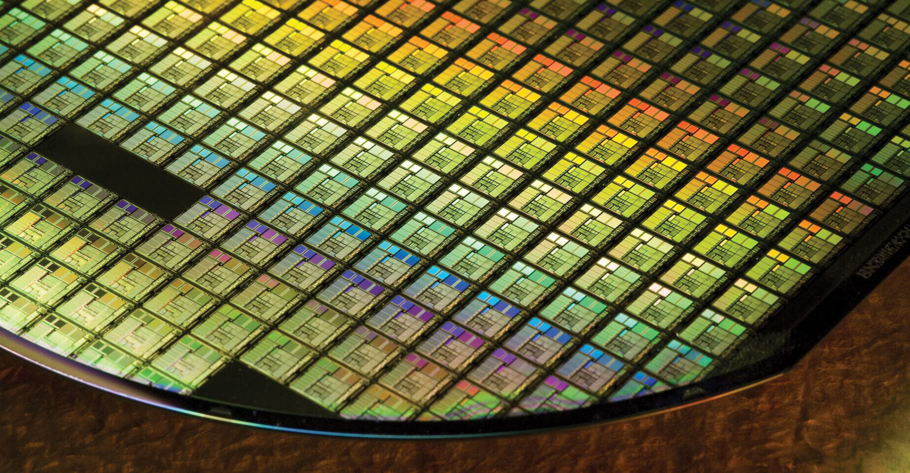
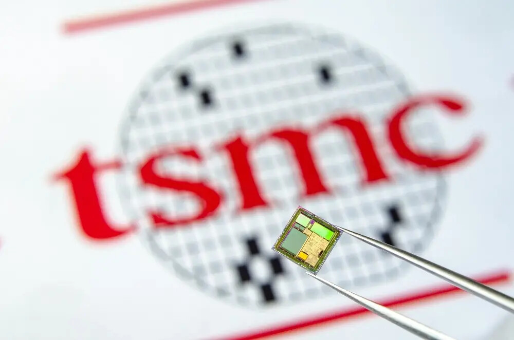
Samsung 5 nm Node Struggles With Yields, Reports Indicate Less Than 50% Yielding

Semiconductor manufacturing is no easy task. Every company in that business knows that, and the hardships of silicon manufacturing have been felt by even the greatest players like Samsung and Intel. Today, according to the latest report from Business Korea, Samsung is again in trouble with its 5 nm node. It has been reported previously that Samsung is struggling with yields of its 5 nm node, however, we didn't know just how much until now. According to the sources over at Business Korea, Samsung's 5 nm semiconductor node is experiencing less than 50% yields. That means, for example, that out of 100 chips manufactured on a single silicon wafer, only half are functional. And that is not good at all.

Usually, for a node to go into high-volume manufacturing (HVM), the yielding rate needs to be around 95%. In case it is not at that level, manufacturing of that node is not very efficient and not very profitable. The V1 Line in Hwaseong, where this Samsung 5 nm is made, uses EUV tools to manufacture the new node. While the yields are currently below 50%, it is expected to improve as Samsung engineers tweak and tune the node and the tools that are running the facility. We can expect to hear more about the yields of this node in the coming months.

Intel Ponte Vecchio GPU to Be Liquid Cooled Inside OAM Form Factor

Intel's upcoming Ponte Vecchio graphics card is set to be the company's most powerful processor ever designed, and the chip is indeed looking like an engineering marvel. From Intel's previous teasers, we have learned that Ponte Vecchio is built using 47 "magical tiles" or 47 dies which are responsible either for computing elements, Rambo Cache, Xe links, or something else. Today, we are getting a new piece of information coming from Igor's LAB, regarding the Ponte Vecchio and some of its design choices. For starters, the GPU will be a heterogeneous design that consists out of many different nodes. Some parts of the GPU will be manufactured on Intel's 10 nm SuperFin and 7 nm technologies, while others will use TSMC's 7 nm and 5 nm nodes. The smaller and more efficient nodes will probably be used for computing elements. Everything will be held together by Intel's EMIB and Foveros 3D packaging.

Next up, we have information that this massive Intel processor will be accountable for around 600 Watts of heat output, which is a lot to cool. That is why in the leaked renders, we see that Intel envisioned these processors to be liquid-cooled, which would make the cooling much easier and much more efficient compared to air cooling of such a high heat output. Another interesting thing is that the Ponte Vecchio is designed to fit inside OAM (OCP Accelerator Module) form factor, an alternative to the regular PCIe-based accelerators in data centers. OAM is used primarily by hyper scalers like Facebook, Amazon, Google, etc., so we imagine that Intel already knows its customers before the product even hits the market.

AMD Zen 4 and RDNA3 Architectures Launching Around the Same Time in 2022

AMD is expected to debut its next-generation "Zen 4" microarchitecture and RDNA3 graphics architectures around the same time, in 2022, according to internal company roadmaps seen by Broly_X1 on Twitter, who has leaked AMD roadmaps before. The "Zen 4" microarchitecture in particular sees AMD debut processors based on the 5 nm silicon fabrication process, and the company's first implementation of an EUV node. With "Zen 4" in 2022, the company could target a so-called "Zen 3+" microarchitecture launch later in 2021, which combines the "Zen 3" CCD with 64 MB of 3D Vertical Cache, a feature that enables a 15% gaming performance uplift, the company claims.

The RDNA3 graphics architecture could see a greater deal of effort toward improving real-time raytracing performance, with more fixed-function hardware dedicated to raytracing. The architecture could see an even bigger generational performance uplift than the one seen between RDNA and RDNA2, according to a PCGamesN report. Across the fence, "Zen 4" and RDNA3 will be squaring off against Intel's "Meteor Lake" and NVIDIA's "ADA Lovelace" architectures, respectively. RDNA3 finishes tape-out toward the end of 2021, as the 5 nm EUV node is already available to AMD for prototyping.

TSMC 4nm Production Hit By... A Full Quarter Advance?

Here's something that has been sorely missing from tech news: good news. It seems that TSMC's development on the 4 nm manufacturing process is running better than anticipated by the company itself, which has prompted for a full quarter advancement for the test production on TSMC's next miniaturization level. Previously scheduled for test production starting on 4Q 2021, TSMC has announced that it has now moved test production to 3Q 2021.

This could mean an equivalent - or perhaps even better - reduction in volume production and time-to-market, but it's anyone's guess at this point. As notably difficult and onerous as semiconductor development is, problems are more likely to appear than not. 4 nm is expected to bring respectable improvements to the PPA equation for semiconductors over 5 nm - however, TSMC still hasn't disclosed expected gains.

AMD's 2022 Ryzen "Raphael" Zen 4 Processor Packs 20% IPC Gain

AMD's second processor microarchitecture on the Socket AM5 platform, the Ryzen 7000 "Raphael," could introduce a 20% IPC gain over its predecessor, according to a report by Moore's Law is Dead. The processor debuts the company's "Zen 4" microarchitecture, which clocks IPC gains over the rumored "Zen 3+" microarchitecture that the Ryzen 6000 "Rembrandt" processor debuts with, on Socket AM5. The upper limit of AMD's core-counts appear to remain at 16-core for the flagship part. With "Zen 4" CCDs (8-core chiplets) being built on 5 nm, the source predicts a 50% performance/Watt gain. The chips could also introduce AVX-512 support. The Ryzen "Raphael" processor is due for 2022.

AMD and GlobalFoundries Wafer Supply Agreement Now Non-Exclusive, Paves Way for 7nm sIOD

AMD in a filing with the U.S. Securities and Exchange Commission (SEC), revealed that its wafer supply agreement with GlobalFoundries has been amended. Under the new terms, AMD places orders for wafers from GlobalFoundries up to 2024, with purchase targets set for each year leading up to 2024. Beyond meeting these targets, AMD is free from all other exclusivity commitments. The agreement was previously amended in January 2019, setting annual purchase targets for 2019, 2020, and 2021, while beginning a de-coupling between AMD and GlobalFoundries. This enabled the company to source 7 nm (or smaller) chips, such as CCDs and GPUs, from other foundries, such as TSMC, while keeping GlobalFoundries exclusive for 12 nm (or larger) nodes.

The updated wafer supply agreement unlocks many possibilities for AMD. For starters, it can finally build a next-generation sIOD (server I/O die) on a more efficient node than GlobalFoundries 12LP, such as TSMC 7 nm. This transition to 7 nm will be needed as the next-gen "Genoa" EPYC processor could feature future I/O standards such as DDR5 memory and PCI-Express Gen 5, and the switching fabric for these could be too power-hungry on 12 nm. The "Zen 4" CPU core complex dies (CCDs) of "Genoa" are expected to be built on TSMC 5 nm.

TSMC to Execute Bitmain's Orders for 5nm Crypto-Mining ASICs from Q3-2021

TSMC will be manufacturing next-generation 5 nm ASICs for Bitmain. The company designs purpose-built machines for mining crypto-currency, using ASICs. DigiTimes reports that the 5 nm volume production could kick off form Q3-2021. Bitmain's latest Antminer ASIC-based mining machines announced last month were purported to be up to 32 times faster than a GeForce RTX 3080 at mining Ethereum. Recent history has shown that whenever ASICs catch up or beat GPUs at mining, prices of GPUs tend to drop. With no 5 nm GPUs on the horizon for Q3-2021, one really can expect market pressure from crypto-miners to drop off when Antminers gain traction.

Apple M2 Processor is Reportedly in Mass Production

Apple's M1 processors are a big success. When Apple introduced the M1 processors in the MacBook lineup, everyone was impressed by the processor performance and the power efficiency it offered. Just a few days ago, Apple updated its Mac lineup to feature these M1 processors and made it obvious that custom silicon is the way to go in the future. Today, we have information coming from Nikkei Asia, that Apple's next-generation M2 chip has entered mass production and that it could be on the way for as early as July when Apple will reportedly refresh its products. The M2 chip is made inside TSMC's facilities on a 5 nm+ N5P node. While there is no more information coming from the report about the SoC, we can expect it to be a good generational improvement.

Foundry Revenue Projected to Reach Historical High of US$94.6 Billion in 2021 Thanks to High 5G/HPC/End-Device Demand, Says TrendForce

As the global economy enters the post-pandemic era, technologies including 5G, WiFi6/6E, and HPC (high-performance computing) have been advancing rapidly, in turn bringing about a fundamental, structural change in the semiconductor industry as well, according to TrendForce's latest investigations. While the demand for certain devices such as notebook computers and TVs underwent a sharp uptick due to the onset of the stay-at-home economy, this demand will return to pre-pandemic levels once the pandemic has been brought under control as a result of the global vaccination drive. Nevertheless, the worldwide shift to next-gen telecommunication standards has brought about a replacement demand for telecom and networking devices, and this demand will continue to propel the semiconductor industry, resulting in high capacity utilization rates across the major foundries. As certain foundries continue to expand their production capacities this year, TrendForce expects total foundry revenue to reach a historical high of US$94.6 billion this year, an 11% growth YoY.

Rumor: AMD Ryzen 7000 (Raphael) to Introduce Integrated GPU in Full Processor Lineup

The rumor mill keeps crushing away; in this case, regarding AMD's plans for their next-generation Zen designs. Various users have shared pieces of the same AMD roadmap, which apparently places AMD in an APU-focused landscape come their Ryzen 7000 series. we are currently on AMD's Ryzen 5000-series; Ryzen 6000 is supposed to materialize via a Zen 3+ design, with improved performance per watt obtained from improvements to its current Zen 3 family. However, Ryzen 7000-series is expected to debut on AMD's next-gen platform (let's call it AM5), which is also expected to introduce DDR5 support for AMD's mainstream computing platform. And now, the leaked, alleged roadmaps paint a Zen 4 + Navi 2 APU series in the works for AMD's Zen 4 debut with Raphael - roadmapped for manufacturing at the 5 nm process.

The inclusion of an iGPU chip with AMD's mainstream processors may signal a move by AMD to produce chiplets for all of its products, and then integrating them in the final product. You just have to think about it in the sense that AMD could "easily" pair one of the eight-core chiplets from the current Ryzen 5800X, for example, with an I/O die (which would likely still be fabricated with Global Foundries) an an additional Navi 2 GPU chiplet. It makes sense for AMD to start fabricating GPUs as chiplets as well - AMD's research on MCM (Multi-Chip Module) GPUs is pretty well-known at this point, and is a given for future development. It means that AMD needed only to develop one CPU chiplet and one GPU chiplet which they can then scale on-package by adding in more of the svelte pieces of silicon - something that Intel still doesn't do, and which results in the company's monolithic dies.

OpenFive Tapes Out SoC for Advanced HPC/AI Solutions on TSMC 5 nm Technology

OpenFive, a leading provider of customizable, silicon-focused solutions with differentiated IP, today announced the successful tape out of a high-performance SoC on TSMC's N5 process, with integrated IP solutions targeted for cutting edge High Performance Computing (HPC)/AI, networking, and storage solutions.

The SoC features an OpenFive High Bandwidth Memory (HBM3) IP subsystem and D2D I/Os, as well as a SiFive E76 32-bit CPU core. The HBM3 interface supports 7.2 Gbps speeds allowing high throughput memories to feed domain-specific accelerators in compute-intensive applications including HPC, AI, Networking, and Storage. OpenFive's low-power, low-latency, and highly scalable D2D interface technology allows for expanding compute performance by connecting multiple dice together using an organic substrate or a silicon interposer in a 2.5D package.

Intel Could Rename its Semiconductor Nodes to Catch Up with the Industry

In the past few years, Intel has struggled a lot with its semiconductor manufacturing. Starting from the 10 nm fiasco, the company delayed the new node for years and years, making it seem like it is never going to get delivered. The node was believed to be so advanced that it was unexpectedly hard to manufacture, giving the company more problems. Low yields have been present for a long time, and it is only recently that Intel has started shipping its 10 nm products. However, its competitor, TSMC, has been pumping out nodes at an amazing rate. At the time of writing, the Taiwanese giant is producing the 5 nm node, with a 4 nm node on the way.

So to remain competitive, Intel would need to apply a new tactic. The company has a 7 nm node in the works for 2023 when TSMC will switch to the 3 nm+ nodes. That represents a marketing problem, where the node naming convention is making Intel inferior to its competitors. To fix that, the company will likely start node renaming and give its nodes new names, that are corresponding to the industry naming conventions. We still have no information how will the new names look like, or if Intel will do it in the first place, so take this with a grain of salt.

TSMC to Enter 4 nm Node Volume Production in Q4 of 2021

TSMC, the world leader in semiconductor manufacturing, has reportedly begun with plans to start volume production of the 4 nm node by the end of this year. According to the sources over at DigiTimes, Taiwan's leading semiconductor manufacturer could be on the verge of starting volume production of an even smaller node. The new 4 nm node is internally referred to as a part of the N5 node generation. The N5 generation covers N5 (regular 5 nm), N5P (5 nm+), and N4 process that is expected to debut soon. And perhaps the most interesting thing is that the 4 nm process will be in high-volume production in Q4, with Apple expected to be one of the major consumers of the N5 node family.

DigiTimes reports that Apple will use the N5P node for the upcoming Apple A15 SoCs for next-generation iPhones, while the more advanced N4 node will find itself as a base of the new Macs equipped with custom Apple Silicon SoCs. To find out more, we have to wait for the official product launches and see just how much improvement new nodes bring.

ASML Finishes Development of EUV Pellicles for Greater Sub-7nm Yields

ASML has finally finished development of EUV (Extreme Ultra Violet) pellicles to be employed in manufacturing processes that use the most energetic frequency of visible light to etch semiconductors onto wafers. Pellicles have been used for decades in the industry, and they are basically ultra-thin membranes that protect photomasks during the etching process - impeding particles from depositing in the substrate, which could lead to defects at the wafer level for every subsequent patterning that is laid on top of the impurity. Manufacturers such as TSMC have deployed EUV-powered manufacturing processes, but they have had to toil with potentially lower yields and increased costs with wafer analysis so as to reduce chances of defects appearing.

It's been a long time coming for EUV-capable pellicles, because these have different requirements compared to their traditional, non-EUV counterparts. However, once they are available on the market, it's expected that all semiconductor manufacturers with bleeding-edge manufacturing processes integrate them into their production flows. These will allow for better yields, which in turn should reduce overall pricing for the manufacturing processes. As an example, these EUV masks could be deployed on TSMC's 7 nm, 6 nm, 5 nm, and so on and so on. Other players other than ASML are also finishing their pellicle design, so the industry will have multiple options to integrate into their processes.

TSMC to Start 3 nm Node Production This Year

Taiwan Semiconductor Manufacturing Company (TSMC), the leading provider of semiconductors, is supposed to start 3 nm node production this year. While Samsung, one of the top three leading semiconductor foundries, has been struggling with the pandemic and delayed its 3 nm node for 2022, TSMC has managed to deliver it this year. According to a report, the Taiwanese semiconductor giant is preparing the 3 nm node for the second half of this year, with the correct date of high-volume product unknown. The expected wafer capacity for the new node is supposed to be around 30,000 wafers per month, with capacity expansion expected to hit around 105,000 wafers per month in 2023. This is similar to 5 nm's current numbers of 105,000 wafers per month output, which was 90,000 just a few months ago in Q4 2020. One of the biggest customers of the upcoming 3 nm node is Apple.

AMD "Genoa" Expected to Cram Up to 96 Cores, MCM Imagined

AMD's next-generation EPYC enterprise processor that succeeds the upcoming 3rd Gen EYPIC "Milan," codenamed "Genoa," is expected to be the first major platform update for AMD's enterprise platforms since the 2017 debut of the "Zen" based "Naples." Implementing the latest I/O interfaces, such as DDR5 memory and PCI-Express gen 5.0, the chip will also increase CPU core counts by 50% over "Milan," according to ExecutableFix on Twitter, a reliable source with rumors from the semiconductor industry. To enable the goals of new I/O and increased core counts, AMD will transition to a new CPU socket type, the SP5. This is a 6,096-pin land grid array (LGA), and the "Genoa" MCM package on SP5 is imagined to be visibly larger than SP3-generation packages.

With the added fiberglass substrate real-estate, AMD is expected to add more CPU chiplets to the package, and ExecutableFix expects the chiplet count to be increased to 12. AMD is expected to debut the "Zen 4" microarchitecture in the enterprise space with "Genoa," with the CPU chiplets expected to be built on the 5 nm EUV silicon fabrication node. Assuming the chiplets still only pack 8 cores a piece, "Genoa" could cram up to 96 cores per socket, or up to 192 logical processors, with SMT enabled.

Revenue of Top 10 Foundries Expected to Increase by 20% YoY in 1Q21 in Light of Fully Loaded Capacities, Says TrendForce

Demand in the global foundry market remains strong in 1Q21, according to TrendForce's latest investigations. As various end-products continue to generate high demand for chips, clients of foundries in turn stepped up their procurement activities, which subsequently led to a persistent shortage of production capacities across the foundry industry. TrendForce therefore expects foundries to continue posting strong financial performances in 1Q21, with a 20% YoY growth in the combined revenues of the top 10 foundries, while TSMC, Samsung, and UMC rank as the top three in terms of market share. However, the future reallocation of foundry capacities still remains to be seen, since the industry-wide effort to accelerate the production of automotive chips may indirectly impair the production and lead times of chips for consumer electronics and industrial applications.

TSMC has been maintaining a steady volume of wafer inputs at its 5 nm node, and these wafer inputs are projected to account for 20% of the company's revenue. On the other hand, owing to chip orders from AMD, Nvidia, Qualcomm, and MediaTek, demand for TSMC's 7 nm node is likewise strong and likely to account for 30% of TSMC's revenue, a slight increase from the previous quarter. On the whole, TSMC's revenue is expected to undergo a 25% increase YoY in 1Q21 and set a new high on the back of surging demand for 5G, HPC, and automotive applications.

TSMC to Put Away More Capacity for Automotive Industry if Possible

TSMC is one of the world's biggest semiconductor manufacturers, and the company is currently the leading provider of the newest technologies like 5 nm and 3 nm, along with advanced packaging. So far, TSMC's biggest customers have included Apple, NVIDIA, AMD, etc., where the company has mainly produced chips for mobile phones and PCs/Servers. However, Taiwan's Economics Ministry has announced that they have spoken to TSMC and have reached an agreement that the company will be putting away some additional capacity for the automotive industry, specifically for the production of automotive chips. The reason for this push is the increasing shortage of semiconductors for automakers, experienced due to the Trump administration sanctions against key Chinese chip factories.

TSMC has stated that "Other than continuously maximizing utilization of our existing capacity, Dr. Wei also confirmed in our investors' conference that we are working with customers closely and moving some of their mature nodes to more advanced nodes, where we have a better capacity to support them". The company also states that their capacities are fully utilized for now, however, TSMC has ensured ministry that "if production can be increased by optimizing production capacity, it will cooperate with the government to regard automotive chips as a primary application." That means that TSMC will not decrease any existing capacity, but rather just evaluate any increased capacity for automotive chip production.

Industry R&D Spending To Rise 4% After Hitting Record in 2020: IC Insights

Research and development spending by semiconductor companies worldwide is forecast to grow 4% in 2021 to $71.4 billion after rising 5% in 2020 to a record high of $68.4 billion, according to IC Insights' new 2021 edition of The McClean Report—A Complete Analysis and Forecast of the Integrated Circuit Industry. Total R&D spending by semiconductor companies is expected to rise by a compound annual growth rate (CAGR) of 5.8% between 2021 and 2025 to $89.3 billion.

When the world was hit by the Covid-19 virus health crisis in 2020, wary semiconductor suppliers kept a lid on R&D spending increases, even though total semiconductor industry revenue grew by a surprising 8% in the year despite the economic fallout from the deadly pandemic. Semiconductor R&D expenditures as a percentage of worldwide industry sales slipped to 14.2% in 2020 compared to 14.6% in 2019, when research and development spending declined 1% and total semiconductor revenue fell 12%. Figure 1 plots semiconductor R&D spending levels and the spending-to-sales ratios over the past two decades and IC Insights' forecast through 2025.

AMD Talks Zen 4 and RDNA 3, Promises to Offer Extremely Competitive Products

AMD is always in development mode and just when they launch a new product, the company is always gearing up for the next-generation of devices. Just a few months ago, back in November, AMD has launched its Zen 3 core, and today we get to hear about the next steps that the company is taking to stay competitive and grow its product portfolio. In the AnandTech interview with Dr. Lisa Su, and The Street interview with Rick Bergman, the EVP of AMD's Computing and Graphics Business Group, we have gathered information about AMD's plans for Zen 4 core development and RDNA 3 performance target.

Starting with Zen 4, AMD plans to migrate to the AM5 platform, bringing the new DDR5 and USB 4.0 protocols. The current aim of Zen 4 is to be extremely competitive among competing products and to bring many IPC improvements. Just like Zen 3 used many small advances in cache structures, branch prediction, and pipelines, Zen 4 is aiming to achieve a similar thing with its debut. The state of x86 architecture offers little room for improvement, however, when the advancement is done in many places it adds up quite well, as we could see with 19% IPC improvement of Zen 3 over the previous generation Zen 2 core. As the new core will use TSMC's advanced 5 nm process, there is a possibility to have even more cores found inside CCX/CCD complexes. We are expecting to see Zen 4 sometime close to the end of 2021.

TrendForce: TSMC to Mass-Produce Select Intel Products, CPUs Starting 2021

According to a market analysis from TrendForce, Intel's manufacturing efforts with TSMC will go way beyond a potential TSMC technology licensing for that company's manufacturing technology to be employed in Intel's own fabs. The market research firm says that Intel will instead procure wafers directly from TSMC, starting on 2H2021, in the order of 20-25% of total production for some of its non-CPU products. But the manufacturing deal is said to go beyond that, with TSMC picking up orders for Intel's Core i3 CPUs in the company's 5 nm manufacturing node - one that Intel will take years to scale down to on its own manufacturing capabilities.

According to TrendForce, that effort will scale upwards with TSMC manufacturing certain allotments of Intel's midrange and high-end CPUs using the semiconductor manufacturer's 3 nm technology in 2022. TrendForce believes that increased outsourcing of Intel's product lines will allow the company to not only continue its existence as a major IDM, but also maintain and prioritize in-house production lines for chips with high margins, while more effectively spending CAPEX on advanced R&D due to savings on fabrication technology scaling - fewer in-house chips means lower needs for investment in capacity increases, which would allow the company to sink the savings into further R&D. The move would also allow Intel to close the gap with rival AMD's manufacturing advantages in a more critical, timely manner.

Apple M1 & A14 Die Shot Comparison Shows Differences in SoC Design

When Apple first announced the M1, questions arose about the differences between it and the A14 chip which both share many architectural features and are both manufactured on TSMC's 5 nm process. Semiconductor analysis firm TechInsights has recently published die photos of the two processors and a summary of the changes.

The M1 features four high-performance Firestorm cores and four energy-efficient IceStorm cores for a total of eight CPU cores. The A14 only features six CPU cores with two high-performance Firestorm cores and four energy-efficient IceStorm cores. The M1 includes doubles the amount of GPU cores and DDR interfaces then found on the A14. The M1 also incorporates silicon not found on the A14 including the Apple T2 security processor and other controllers. These additions result in a die size 37% larger than the A14.

NVIDIA's Next-Gen Big GPU AD102 Features 18,432 Shaders

The rumor mill has begun grinding with details about NVIDIA's next-gen graphics processors based on the "Lovelace" architecture, with Kopite7kimi (a reliable source with NVIDIA leaks) predicting a 71% increase in shader units for the "AD102" GPU that succeeds the "GA102," with 12 GPCs holding 6 TPCs (12 SMs), each. 3DCenter.org extrapolates on this to predict a CUDA core count of 18.432 spread across 144 streaming multiprocessors, which at a theoretical 1.80 GHz core clock could put out an FP32 compute throughput of around 66 TFLOP/s.

The timing of this leak is interesting, as it's only 3 months into the market cycle of "Ampere." NVIDIA appears unsettled with AMD RDNA2 being competitive with "Ampere" at the enthusiast segment, and is probably bringing in its successor, "Lovelace" (after Ada Lovelace), out sooner than expected. Its previous generation "Turing" architecture saw market presence for close to two years. "Lovelace" could leverage the 5 nm silicon fabrication process and its significantly higher transistor density, to step up performance.

NVIDIA to Introduce an Architecture Named After Ada Lovelace, Hopper Delayed?

NVIDIA has launched its GeForce RTX 3000 series of graphics cards based on the Ampere architecture three months ago. However, we are already getting information about the next-generation that the company plans to introduce. In the past, the rumors made us believe that the architecture coming after Ampere is allegedly being called Hopper. Hopper architecture is supposed to bring multi-chip packaging technology and be introduced after Ampere. However, thanks to @kopite7kimi on Twitter, a reliable source of information, we have data that NVIDIA is reportedly working on a monolithic GPU architecture that the company internally refers to as "ADxxx" for its codenames.

The new monolithically-designed Lovelace architecture is going make a debut on the 5 nm semiconductor manufacturing process, a whole year earlier than Hopper. It is unknown which foundry will manufacture the GPUs, however, both of NVIDIA's partners, TSMC and Samsung, are capable of manufacturing it. The Hopper is expected to arrive sometime in 2023-2024 and utilize the MCM technology, while the Lovelace architecture will appear in 2021-2022. We are not sure if the Hopper architecture will be exclusive to data centers or extend to the gaming segment as well. The Ada Lovelace architecture is supposedly going to be a gaming GPU family. Ada Lovelace, a British mathematician, has appeared on NVIDIA's 2018 GTC t-shirt known as "Company of Heroes", so NVIDIA may have already been using the ADxxx codenames internally for a long time now.

TSMC Ends Its Volume Discounts For the Biggest Customers, Could Drive Product Prices Up

Taiwan Semiconductor Manufacturing Company (TSMC), one of the largest semiconductor manufacturers in the world, is reportedly ending its volume discounts. The company is the maker of the currently smallest manufacturing nodes, like 7 nm and 5 nm. For its biggest customers, TSMC used to offer a discount - when you purchase 10s or 100s of thousands of 300 mm (12-inch) wafers per month, the company will give you a deal of a 3% price decrease per wafer, meaning that the customer is taking a higher margin off a product it sells. Many of the customers, like Apple, NVIDIA, and AMD, were a part of this deal.

Today, thanks to a report from the Taiwanese Central News Agency, TSMC is terminating this type of discount. Now, every customer will pay full price for the wafer, without any exceptions. For now, it is unclear what drove that decision at TSMC's headquarters, but the only thing that we could think is that the demand is too high to keep up with the discounts and the margins are possibly lower. What this means for consumers is a possible price increase in products that are manufactured at TSMC's facilities. The consumer market is already at a drought of new PC components like CPUs and GPUs due to high demand and scalping. This could contribute a bit to the issue, however, we do not expect it to be of any major significance.
Return to Keyword Browsing
May 21st, 2024 20:26 EDT change timezone

New Forum Posts

Popular Reviews

Controversial News Posts