Friday, September 11th 2009

AMD Cypress ''Radeon HD 5870'' Stripped
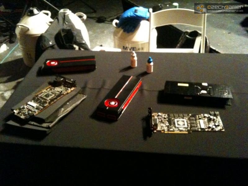
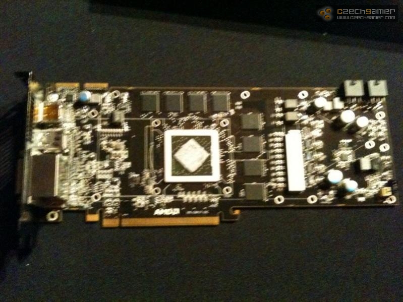
Here are the first pictures of the obverse side of Cypress' PCB, and the first pictures of the centre of attraction: the AMD Cypress GPU. CzechGamer dissembled two Cypress "Radeon HD 5870" cards for a quick blurrycam photo-session. The PCB shot reveals quite a bit about Cypress, particularly about the GPU.
To begin with, the GPU is AMD's overhaul on transistor counts, and a bold work of engineering on the 40 nm manufacturing process, given the kind of problems foundry partners had initially. Apparently they seem to have recovered with most of them, as AMD's AIB partners are coming up with new products based on the 40 nm RV740 GPU on a weekly basis. The package holds a "diamond-shaped" die that is angled in a way similar to RV740, RV730, or more historically, the R600. The seemingly huge die measures 338 mm² (area), and for 40 nm, it translates to "huge", and is vindicated by the transistor count of ~2.1 billion. In contrast, AMD's older flagship GPU, the RV790 holds 959 million, and NVIDIA's GT200 holds 1.4 billion. The PCB has three distinct areas: the connectivity, processing, and VRM. To fuel the GPU is a high-grade 4 phase digital PWM power circuit, while the PCB has placeholders for an additional vGPU phase. The 8 (or 16 on the 2 GB model) memory chips, is powered by a 2 phase circuit. Power is drawn from two 6-pin PCI-Express power connectors, but there seems to be a placeholder for two more pins, i.e., to replace one of those 6-pin connectors with an 8-pin one. Bordering the GPU on two sides are the 8 GDDR5 memory chips, which AMD calls says is generation ahead of present GDDR5, and supports reference frequencies as high as 1300 MHz (2600 MHz DDR, 5.20 GHz effective). In the 2 GB variant, 8 more chips seat on the other side of the PCB. This is what perhaps, the backplate is intended to cool. On the connectivity portion of it, are the two CrossFire connectors, DisplayPort, HDMI and a cluster of two DVI-D connectors. There has been a raging debate about how adversely the small air vent would affect the card, but AMD is promising some energy efficiency breakthroughs, plus given how roomy the card is, the vent seems sufficient.

Finally, information from ArabHardware.net suggests a pricing model on three of the first SKUs based on Cypress: HD 5870 2 GB, HD 5870 1 GB, and HD 5850 1 GB. All three use the same GPU and memory standard (GDDR5), but differ in clock speeds and GPU configurations. While HD 5870 sports 1600 stream processors, 80 TMUs, and 32 ROPs, HD 5850 has 1440 stream processors, 72 TMUs, and 32 ROPs. Although 32 ROPs puzzles us for a 256-bit wide memory interface, we suspect low-level design changes that make "32 ROPs" more of an effective count than an absolute count. While HD 5870 features over 800 MHz core clock and 5.20 GHz memory, its little sibling has over 700 MHz core clock and 4.40 GHz memory. Price points expected are US $449 for Radeon HD 5870 2 GB, $399 for HD 5870 1 GB, and $299 for HD 5850. AMD is expected to announce all three models on the coming 23rd. You'll be able to find them at your favourite computer store a little later, availability is a certainty by the time you're ready to buy Windows 7. AMD's newest products will be more than ready to squat under X-mas trees all over.
Sources:
Czech Gamer, Arab Hardware
To begin with, the GPU is AMD's overhaul on transistor counts, and a bold work of engineering on the 40 nm manufacturing process, given the kind of problems foundry partners had initially. Apparently they seem to have recovered with most of them, as AMD's AIB partners are coming up with new products based on the 40 nm RV740 GPU on a weekly basis. The package holds a "diamond-shaped" die that is angled in a way similar to RV740, RV730, or more historically, the R600. The seemingly huge die measures 338 mm² (area), and for 40 nm, it translates to "huge", and is vindicated by the transistor count of ~2.1 billion. In contrast, AMD's older flagship GPU, the RV790 holds 959 million, and NVIDIA's GT200 holds 1.4 billion.

163 Comments on AMD Cypress ''Radeon HD 5870'' Stripped
And if you noticed, I said something positive also...but you do only tend to notice when people say negative things about ATi...but you are an ATi fanboy so it is expected I guess...:shadedshuI don't care about G300, this isn't a topic about G300.
The large die size is a good thing. It means ATi packed a lot of shit in there, hopefully that means awesome performance. And it means 40nm has matured to the point that it can handle large die sizes like this.
anyway
these should be close
HD5870
GPU:RV870XT
Core Clock:850 Mhz
Shader Clock:850 Mhz
Memory Clock:1300 Mhz
Pixel Fill Rate:27200 MPixels/sec
Texture Fill Rate:68000 MTexels/sec
HD5850
GPU:RV870
Core Clock:750 Mhz
Shader Clock:750 Mhz
Memory Clock:1100 Mhz
Pixel Fill Rate:24000 MPixels/sec
Texture Fill Rate:54000 MTexels/sec
HD4870X2
GPU:RV770X2
Core Clock:750 Mhz
Shader Clock:750 Mhz
Memory Clock:1800 Mhz
Pixel Fill Rate:24000 MPixels/sec
Texture Fill Rate:60000 MTexels/sec
HD4890
GPU:RV770XT
Core Clock:850 Mhz
Shader Clock:850 Mhz
Memory Clock:975 Mhz
Pixel Fill Rate:13600 MPixels/sec
Texture Fill Rate:34000 MTexels/sec
I typically build a new rig every summer/fall for myself alternating between Intel and AMD systems. I was actually excited to invest in i7 860/p55/single 295 this time around now I am considering waiting to see if an HD 5870x2 comes out! If it does I will just wait for the Leo platform to be released in May. I haven’t bought a Radeon card since the x800 so this is kind of exciting!
Should be fine and dandy.
We all know that the 8000 series were the first G Cards to support DX10 and they didn't preform well in these games to be honest so I don't think that these new DX11 cards will do better than their predecessors , not to mention that we will probably see the first DX11 game after 2 or 3 years.
I'm still gonna WC it and see what NV has to say later on ;).
Most of the early "DX11" games will be DX10 games with a few generally unnoticable additions. What DX version the game uses, or even what version the card supports, isn't really important to me. Good gameplay is what is important, and the horsepower of the card is what I'm worried about.With power saving features, I would believe 27w at idle, but I don't care about idle, even the current ATi cards are quiet at idle. And at 185w at load, you are looking at more than a GTX295.:eek:
And I have seen the cooler design, and the two openning at the front of the card are decoration only it seems. There is no way they are intakes, as they face the exhaust part of the fan. And it looks like the fan is actually blocked off from the fan entirely. If they aren't, then the cool air being sucked in from the fan is just being exhausted right out the holes, not cooling anything, making them useless. Either way, they don't help the situation with the extremely small exhaust at the back of the card, this will limit airflow, causing higher temps, and force the fan to work harder and louder.
We will have to see when the card is actually released, but that is just my opinion after seeing the pictures so far. And yes, I'm well aware that this might not be the final design, and they might reduce or re-arrange the connectors on the card.
i want to see benches right now :cry:, please
Also, those with the card are claiming it's 50% faster than GTX285.
Its been a while since I checked the website (I'm shitting you not), I don't see much graphical difference between the DX10 games and Dirt 2 so in my opinion it's not DX11 unless it has a graphical improvement I mean big improvement not minor changes which you won't be able to notice.
Back to topic, when do you think we will see the first accurate benchmarks of these cards ?
And isn't a GTX295 about 50% faster than a GTX285?