Monday, September 6th 2010

Picture of AMD ''Cayman'' Prototype Surfaces
Here is the first picture of a working prototype of the AMD Radeon HD 6000 series "Cayman" graphics card. This particular card is reportedly the "XT" variant, or what will go on to be the HD 6x70, which is the top single-GPU SKU based on AMD's next-generation "Cayman" performance GPU. The picture reveals a card that appears to be roughly the size of a Radeon HD 5870, with a slightly more complex-looking cooler. The PCB is red in color, and the display output is slightly different compared to the Radeon HD 5800 series: there are two DVI, one HDMI, and two mini-DisplayPort connectors. The specifications of the GPU remain largely unknown, except it's being reported that the GPU is built on the TSMC 40 nm process. The refreshed Radeon HD 6000 series GPU lineup, coupled with next-generation Bulldozer architecture CPUs and Fusion APUs are sure to make AMD's lineup for 2011 quite an interesting one.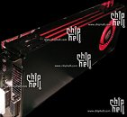
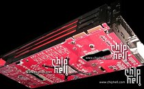
Update (9/9): A new picture of the reverse side of the PCB reveals 8 memory chips (256-bit wide memory bus), 6+2 phase VRM, and 6-pin + 8-pin power inputs.
Source:
ChipHell


118 Comments on Picture of AMD ''Cayman'' Prototype Surfaces
And maybe that driver change was a pre-emptive strike in preparation for these cards...:twitch:
I'm still more interested in Bulldozer-based Fusion chips though. The combination of a that cpu, plus these add-in cards(if less complex, but higher-order math), might be the huge boost that pushes AMD back into the performance lead when it comes to 3D.To me, it seems that that only really suits the HPC crowd, and older-style game programming though. Largon's mention of Furmark kinda illustrates that very well, IMHO. No game pushes HD5-series like Furmark...the math in Furmark is very simple, and games are not.
I'm looking for a few other specific changes, and AMD really might have a huge winner here...I guess time will tell.
512bit bus in 40nm: 170mm^2/(80nm/40nm)^2 = 42.5mm^2 ~10%
256bit bus in 40nm: 36mm^2/(55nm/40nm)^2 = 19.4mm^2
which overall a 512bit bus will only take about 12% if in current cypress's 334mm^2 die. it isn't really that big.
5770 is also a 8 ram chip card but it only had 128bit so basically chip number is nothing to do with bus like nvidia's design for its card. just to remind you x2900xt is ALSO have only 8 chip as well. for what you said about 16x 12x ram IC was nvidia's exclusive architecture which amd's card can add as much ram as possible without concerning ram bus and ram controller.
2900XT, truly, is only 256-bit. It was considered 512-bit becuase it had 256-bit to the "ringstops", and then 256-bit from "ringstop" to mem IC's. because these two busses could operate independantly, both can have data in-flight, it was effectively given 512-bits of data transfer...but the memory bus, is NOT truly 512bit.
You are ignoring that AMD is a business, and as such, profitability is concern #1. As such, changes that increase pricing, must have a real tangible benefit, or they wil lbe cut from the design...Cypress, at first, was a much larger chip than we got...for exactly this reason. With that in mind, they can make better, more PRICE EFFECTIVE use of that die space, than adding 512-bit memory control.
So, I can say that the pictured card is 256-bit only...due to ICs...the only other option, based on available parts, is a 128-bit GPU, and that would not suffice for a high-end SKU.
Prepare to say hello to 5-10GHz GDDR5 chippery.Only in theory. Reality is less ideal.
Scratch that. You're in a whole wrong ballpark.
You're comparing GDDR3/4 memctrl and GDDR5. GDDR5 uses some ~20% more pins (area), so 512bit GDDR5 ctrl is larger than 512bit GDDR3/4 ctrl. And what's worse, MEMIO does not scale linearly with fab process. It actually scales hardly at all on today's process'. The problem is IO pads, that is, the solder balls between IC and chip carrier are sized what they are and there's no way shrinking the distance between 'em. Difference between IO pads on, say, a 90nm chip and 32nm chip is nowhere near as large as one would think.That's just plain wrong.
Bus width is dictated by number of memory chips and bit width of those chips. Any and all GDDR3/4/5 chips come only up to 32bit wide. HD2900XT has 16 chips. And that's a fact.
I have two HD2900XT cards here so I can point 'em to you if you want to argue.
There was eight ringstops of which each was a dualchannel controller (64bit) and each ringstop connected to two other stops with 1024bit bidirectional bus (512bit˄ + 512bit˅).
but that isn't even 100% true, as there is a ringstop for PCI-E, and a ringstop for Crossfire connector. But yes, 8 for memory control.
4D is what is coming on the 6 series.
Like I said in the 6k thread, expect a shader setup like what nVidia changed to for Fermi (not exact but similar). Shaders will be grouped with parts of the DX11 pipeline including the tessellation part since triangles/clock is what will define a DX11 gpu. Of course you will need to group shaders with these so as to work as units together.
Kind of like a multi core cpu, but not really.
It is said that DP is more flexible and what-so-ever + free, so it would seem that it's quite possible.
DVI*2+HDMI+miniDP*2 and 6+8pin 2GB GDDR5 860mhz