Saturday, November 12th 2011

AMD Justifies Using Liquid Chamber Tech On Upcoming 7900-Series Cards

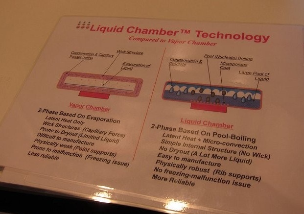
videocardz.com brings us a photo showing the benefits of AMD's new liquid chamber technology over the standard vapour chamber technology used in current heatpipe cooling solutions. There's quite a few benefits, some of which are no drying out, physical robustness and greater reliability. Indeed, can you imagine the disastrous effect on your graphics card of having the cooling system spring a leak during an intense gaming session? Doesn't bear thinking about… Certainly the era of having to replace your graphics card's shrill and inefficient cooler with a high performance aftermarket one are long over, as stock coolers are now generally of very good quality. The liquid chamber system will be used by all AMD's partners who stick to the reference design. Check out the photo for the full info.
Add your own comment

54 Comments on AMD Justifies Using Liquid Chamber Tech On Upcoming 7900-Series Cards

#26
pantherx12
John DoeI think you need a reality check. Both the 3870 and the 2900 had 16 ROP's, which is why they performed the same. Those two were based on the same thing.

www.gpureview.com/show_cards.php?card1=518&card2=547

About power draw, no the 6970 doesn't pull more than a 2900. The 2900 pulled a lot of power and worked hot due to it's ineffective design. Pheaderus has his card OC'ed (against his 4870 with 150W TDP) and Guru3D is running FurMark so do the thinking.

The 6970 wouldn't run hotter with a HD 2900 sink, this is getting nonsensical but anyway, the 6970 only has a heatsink with fins, while the HD 2900 has a heatpiped sink.

As for 6970 against 570, yes, that's what it meant. The 570 has more transistors, is rated to pull less power yet it pulls more on Guru3D. With both under the SAME conditions.
Just a heatsink? Dude you really all those fins are embedded into a vapour chamber right? Basically big heatpipe? (Note the fill point bottom right)


Double checking the rop thing my memory could be hazy.

Regarding power consumption have a look at this, bare in mind the 2900xt powerconsumption is total system power consumption where as the 6970 is just the card.
2900xt


6970


And 9800gt systempower consumption as it's included in the 6970s card power draw so you can get a better reference
Posted on Reply
#27
shb-
Those slides really abuses vapor chamber. Hope this is just to make liquid chamber look better, because i use vapor chamber cooling solution on my card.
Posted on Reply
#28
InnocentCriminal
Resident Grammar Amender
Sounds like the ICE units in Shuttles to me.

Hopefully it'll be quiet.
Posted on Reply
#29
mediasorcerer
It probably works in any position in relation to gravitational forces, just like vapour chamber, it may not matter how the chamber is positioned as the precipitation will work anyway. The heat may be transferred through the chamber itself rather than the liquid so much.[im guessing go easy!]
=latent heat & micro convection [may not be subject to gravity at the micro level]?,micro porous coat= theres a clue i think.
Also, this diagram and info may be innnacurate to a degree, due to patents infringements or intellectual property rights violations and that sort of thing, they wouldnt give theyre new idea away just like that would they, else it may be plageurised etc>?
Posted on Reply
#30
de.das.dude
Pro Indian Modder
i am thinking since the card is place upside down, how will the liquid come in contact with the core surface ??
Posted on Reply
#31
mediasorcerer
de.das.dudei am thinking since the card is place upside down, how will the liquid come in contact with the core surface ??
Das i think everyones thought the same thing and me too mate, but obviously they have it working somehow regardless of the orientation of the chamber[like vapour chambers do too?], perhaps since its on a "micro" level it may not be subject to the same gravitational forces ?or it may be done in a vacuum , maybe the liquid itself does not transfer the heat as much as the outer chamber , and the micro porous material works in any rotation etc,just thinking but good question really.:)

we may never know haha! i bet the diagrams are wrong somehow, or somethings left out, to stop people stealing the idea , they all do that to protect there intellectual property.
Posted on Reply
#32
Super XP
I have a feeling AMD plans on upping the GPU and Memory clock speeds by a lot and want to ensure they can by using this method of cooling. This should easily work great.
Posted on Reply
#33
badtaylorx
so essentially the liquid chamber is just a better heat spreader......no

perhaps they should combine this WITH heat pipe tech

liquid chamber to bring the heat up off the chip

and heat pipes to spread it out over a larger surface area
Posted on Reply
#34
AsRock
TPU addict
pantherx12I'm not man, yes if they used the exact same design but used a smaller process then tdp will be reduced, but this rarely happens, people take advantage of the smaller size and pack twice as much in as before leading us back to where we were before in terms of TDP and powerdraw.

Might have grabbed the powerdaw rather than TDP but source said it's TDP, the 580 if my source is right has a 244W TDP. The TDP of a 2900xt was 215W.

See what I mean? Heat output stays around the same level for top end cards because like I said they go for double the speed not half the size.


The 3870 was pretty much the same as a 2900xt ( infact it has less transistors, lower rop count) yet was on a smaller process hence it's powerdraw being much lower than that of the 2900xt.


If we were just doing powerdraw ( according to geeks3d)


8800 Ultra 175w 90nm 681M Transistors
9800 GTX+ 141w 55nm 754M Transistors
GTS 285 204w 40nm 1400M Transistors
GTX 480 260w (peak 3D) 40nm 3200M Transistors
GTX 560 Ti 205w (peak 3D) 40nm 1950M Transistors
GTX 580 280w (peak 3D) 40nm 3000M Transistors

2900xt 215w 90nm 700M Transistors
HD 3870 105w 55nm 666M Transistors
HD 4870 157w 55nm 956M Transistors
HD 5870 188w 40nm 2154M Transistors
HD6870 151w 40nm 1700M Transistors
HD 6970 250 (PowerTune +20%) 40nm 2640M Transistors

Hell the 6970 is hotter and more powerhungry then a 2900xt


Fab process just affects how much they can fit in one space, the voltage requirement is reduced as well so yes you can get a lower TDP but not all the time design as it depends on the design of the card it's self.


Excuse me if I've got any odd typos or if this is a bit rambling, no sleep makes panther something something.


*edit* added Nvidia cards, took me longer to collate data.
Well having a 2900XT,4890 then a 6970 they take all about the same power in games although the performance is a totally different thing. Always been between 300W and 370w with all cards.

And the 2900XT was not like the 3870 as the 3870 was 256bit were as the 2900 was 512bit.
Posted on Reply
#35
cdawall
where the hell are my stars
John Doelol? Both, I'm talking about both. If you shrink down a GPU, you'll lower down it's TDP as well. The 3870, although based on a cheaper PCB, pulled half as much power as the HD 2900 after a big die shrink (with the help of better manufactoring as well).
Die size has nothing to do with power consumption. Go look into wattage calcs nothing on there says to type in die size because .9v @ XXXmhz 150w is the same wattage regardless of die size.
Posted on Reply
#36
robal
Pity, that I'll have to pay for that just to strip it away and place waterblock instead.

Why is it that 'watercooled' cards (even if you can find one in stock) are considered "enthusiast rarity" and cost way more than just stock card + 3rdparty waterblock ?

Why is there no choice to buy 'cooler-less' card ?

Aargh...

PS: I support good OEM aircooling solutions... But I hate not being given a choice.
Posted on Reply
#37
pantherx12
AsRockWell having a 2900XT,4890 then a 6970 they take all about the same power in games although the performance is a totally different thing. Always been between 300W and 370w with all cards.

And the 2900XT was not like the 3870 as the 3870 was 256bit were as the 2900 was 512bit.
Cheers man this is what I've been trying to say, and I knew the 2900xt was 512bit, just wasn't 100% :laugh: :toast: ( still similar though same shaders and such like, I think they just pulled out all the bits of 2900 that didn't work)

By the by anyone know why the TPU review says 16x2 for rops is this in-fact the case? Only asking as it's only really TPU I can find it written as a spec :laugh:
Posted on Reply
#38
erocker
*
Where's the part that AMD explains it's justification for using this magical technology? Who knows, maybe it's just cheaper to produce. As far as Accellero Xtreme's, the great thing about those is that they're pretty much compatable with anything. They are a bit pricey, but they'll last over a few generations of GPU's at least. One of the better computer hardware purchases I've made.
Posted on Reply
#40
AsRock
TPU addict
pantherx12Cheers man this is what I've been trying to say, and I knew the 2900xt was 512bit, just wasn't 100% :laugh: :toast: ( still similar though same shaders and such like, I think they just pulled out all the bits of 2900 that didn't work)

By the by anyone know why the TPU review says 16x2 for rops is this in-fact the case? Only asking as it's only really TPU I can find it written as a spec :laugh:
No idea why it would say 2x16 thats weird. I always thought it was just 16 due to it being one gpu..

Power usages are just max of what the card can do and lets face it they don't hit those maxes unless you use BS furmark or alike.

I think the power usages should be done for each game as well but surly take would take much more time. My max system out put for my 775 system was 520w using OCCT but ANY game maxed at 370w.
erockerWhere's the part that AMD explains it's justification for using this magical technology? Who knows, maybe it's just cheaper to produce. As far as Accellero Xtreme's, the great thing about those is that they're pretty much compatable with anything. They are a bit pricey, but they'll last over a few generations of GPU's at least. One of the better computer hardware purchases I've made.
profit ?.. Cheaper ?.. Better for CF ?.. Surly they use these coolers so other companys like XFX Powercooler and such can make a profit from making there own coolers for the cards.. Hence more sales.

I think they are actually doing it as they are trying to keep the same design due
Posted on Reply
#41
Bundy
de.das.dudei am thinking since the card is place upside down, how will the liquid come in contact with the core surface ??
Perplexing issue, unless the cooler is just a series of heat pipes set in a block? Capilliary action might be achieved via grooves.
Posted on Reply
#42
Unregistered
cdawallDie size has nothing to do with power consumption. Go look into wattage calcs nothing on there says to type in die size because .9v @ XXXmhz 150w is the same wattage regardless of die size.
It does. Online PSU calculators are garbage to begin, so they shouldn't be looked at, at all.

Why do you think the 285 peaks to 200W when the 280 peaks 250W, although the 285 has higher clocks? Because it's 55nm over 65nm. Come on.
Posted on Edit | Reply
#43
cdawall
where the hell are my stars
John DoeIt does. Online PSU calculators are garbage to begin, so they shouldn't be looked at, at all.

Why do you think the 285 peaks to 200W when the 280 peaks 250W, although the 285 has higher clocks? Because it's 55nm over 65nm. Come on.
Never said psu calc now did I . I said a thermal calc. The 285 is 55nm lower wattage than the 280's 65nm core go crank the voltages to the same and clock speeds to the same the power consumption/output will be the same. Die package size has ZERO contributions towards thermal effeciency. Newer dies are more effecient ue to lower leakage parts and better designs, which in turn lead to lower voltages. Hell look at new cpu's default wattages are getting closer to the same regardless of die size.
Posted on Reply
#44
Damn_Smooth
I want one now. Would somebody hurry up and build a damn time machine already?
Posted on Reply
#45
AsRock
TPU addict
pantherx12Just a heatsink? Dude you really all those fins are embedded into a vapour chamber right? Basically big heatpipe? (Note the fill point bottom right)
static.techspot.com/articles-info/348/images/Image_12S.jpg

Double checking the rop thing my memory could be hazy.

Regarding power consumption have a look at this, bare in mind the 2900xt powerconsumption is total system power consumption where as the 6970 is just the card.
2900xt
tpucdn.com/reviews/ATI/HD_2900_XT/images/power_peak.gif

6970
tpucdn.com/reviews/HIS/Radeon_HD_6970/images/power_peak.gif
tpucdn.com/reviews/HIS/Radeon_HD_6970/images/power_maximum.gif


And 9800gt systempower consumption as it's included in the 6970s card power draw so you can get a better reference
tpucdn.com/reviews/Zotac/GeForce_9800_GT_Amp_Edition/images/power_peak.gif
Back then if you read the heading to them the 2900XT were unser total system usage and not just the card.. There fore accuracy is wrong, and like i said unless your running a BS program like Furmark power usages are all around the same just that the actual performance has increased.

Like i have noticed one game which is Tiger Woods 08 played it with the 2900XT, 4890 and 6970 and always taking about the same power usage although performance has gained a fair bit. And always been around 290w-330w max with any of the cards.
Posted on Reply
#46
Unregistered
cdawallNever said psu calc now did I . I said a thermal calc. The 285 is 55nm lower wattage than the 280's 65nm core go crank the voltages to the same and clock speeds to the same the power consumption/output will be the same. Die package size has ZERO contributions towards thermal effeciency. Newer dies are more effecient ue to lower leakage parts and better designs, which in turn lead to lower voltages. Hell look at new cpu's default wattages are getting closer to the same regardless of die size.
Well the thermal calculator is built in the PSU one, which is untrustable. The only calculator you should rely on is the one Pheaderus recently did.

www.overclock.net/t/1045231/phaedrus-quickndirty-psu-calculator

Any other is a joke in regards to the values it gives, so I'd take anything a PSU calculator says with a truck of salt. They overexaggerate your needs and advertise 1000W+ units on that site (eXtreme nonsense) for PSU sellers to gain revenue:

www.overclockers.com/forums/showpost.php?p=5725802&postcount=13

Anyway, that's not the topic. What I'm saying is, a lower die size comes in a "smaller" GPU. Bigger GPU = less efficient with higher leakage in theory. That's how manufactoring is improved.

Also, the 285 doesn't have lower volts than the 280. In fact, the 285 was a cheaper to make design that most cards (second rev.) worked around 1.15v, while the 280 functioned around 1v. So that's not how it works.
Posted on Edit | Reply
#47
cdawall
where the hell are my stars
John DoeWell the thermal calculator is built in the PSU one, which is untrustable. The only calculator you should rely on is the one Pheaderus recently did.

www.overclock.net/t/1045231/phaedrus-quickndirty-psu-calculator

Any other is a joke in regards to the values it gives, so I'd take anything a PSU calculator says with a truck of salt. They overexaggerate your needs and advertise 1000W+ units on that site (eXtreme nonsense) for PSU sellers to gain revenue:

www.overclockers.com/forums/showpost.php?p=5725802&postcount=13
NO ONE BUT YOU has even brought up a PSU calc they have nothing to do with what I am talking about.


CPU wattage calc notice the complete and utter lack of die size. This calc is also years and years old now and still correct because this is how wattage of a CPU is calculated. Po = Ps * (Fo/Fs) * (Uo^2/Us^2) is the mathmatical formula for CPU power usage (and in turn GPU) and it will NEVER change.
John DoeAnyway, that's not the topic. What I'm saying is, a lower die size comes in a "smaller" GPU. Bigger GPU = less efficient with higher leakage in theory. That's how manufactoring is improved.
All things equal a larger die is no less efficient. How could it be 1.4B transistors are still 1.4B transistors it does not matter how they get packaged together.
John DoeAlso, the 285 doesn't have lower volts than the 280. In fact, the 285 was a cheaper to make design that most cards (second rev.) worked around 1.15v, while the 280 functioned around 1v. So that's not how it works.
You know what I love your comparison here. the 285 is higher voltage its also higher clocked AND CONSUMES MORE POWER.

Comparing two different GPU's is also stupid PWM is different and that alone could drastically change power consumption. Hell look card to card and you see major variations between designs.
Posted on Reply
#48
Unregistered
cdawallCPU wattage calc notice the complete and utter lack of die size. This calc is also years and years old now and still correct because this is how wattage of a CPU is calculated. Po = Ps * (Fo/Fs) * (Uo^2/Us^2) is the mathmatical formula for CPU power usage (and in turn GPU) and it will NEVER change.
That has nothing to do with what I said. What that calculator calculates is how much power AN OC will pull over stock. It doesn't compare different chips. Compare a Nehalem to a Westmere. A Xeon E5640 has a 80W TDP against the 130W of an i7 920, although it has more cache. Reason? 32nm against 45nm = more mature manufactoring process. Full stop.
cdawallYou know what I love your comparison here. the 285 is higher voltage its also higher clocked AND CONSUMES MORE POWER.
img.techpowerup.org/111113/Capture167.jpg
Comparing two different GPU's is also stupid PWM is different and that alone could drastically change power consumption. Hell look card to card and you see major variations between designs.
No, it doesn't. Wattage meters can be horribly inaccurrate. They aren't calibrated enough to show the exact DC power. AC to DC is converted on the primary of a PSU, so you can't measure it %100 accurate from the wall (even if you measure AC-DC transformation).

The 280 had a higher quality PCB than the 285. It had a Chil controller and so, along with a reference design only. Other hand, 285's were mostly non-ref (second revisio) designs that're cheaper, yes.

However, the 285 has a 185W TDP against the 235W of a 280. So it's a give or take depending on what exactly you're comparing. But one can expect a 285 to pull less power since it was built on a core that worked much cooler with less leakage (powers).
Posted on Edit | Reply
#49
cdawall
where the hell are my stars
John DoeThat has nothing to do with what I said. What that calculator calculates is how much power AN OC will pull over stock. It doesn't compare different chips.
The point was there was no difference between core sizes if there was 65nm would have a different power curve than 45nm and would have to be labeled as such. Point is it doesn't.
John DoeCompare a Nehalem to a Westmere. A Xeon E5640 has a 80W TDP against the 130W of an i7 920, although it has more cache. Reason? 32nm against 45nm = more mature manufactoring process. Full stop.
Its also a specifically binned server chip that was designed to be an 80w TDP chip. The same can be done with a larger die. AMD does it all of the time there are tons of 65/90nm chips rated at the same TDP same clocks etc.
John DoeNo, it doesn't. Wattage meters can be horribly inaccurrate. They aren't calibrated enough to show the exact DC power. AC to DC is converted on the primary of a PSU, so you can't measure it %100 accurate from the wall (even if you measure AC-DC transformation).
So is comparing two different GPU's on two different PCB's while your at it why not throw in a 4870 for comparison that'll make it accurate.
John DoeThe 280 had a higher quality PCB than the 285. It had a Chil controller and so, along with a reference design only. Other hand, 285's were mostly non-ref (second revisio) designs that're cheaper, yes.
Oh wait so the PCB is different and had different VRM. Hmmm I wonder if that might have anything to do with it.
John DoeHowever, the 285 has a 185W TDP against the 235W of a 280. So it's a give or take depending on what exactly you're comparing. But one can expect a 285 to pull less power since it was built on a core that worked much cooler with less leakage (powers).
No it was built on a 55nm core built on a different PCB with different memory etc. way to many variable to make any kind of decision on die size.
Posted on Reply
#50
Unregistered
cdawallThe point was there was no difference between core sizes if there was 65nm would have a different power curve than 45nm and would have to be labeled as such. Point is it doesn't.
There is because manufactoring process gets improved along with a die size decrease. That's why nVidia's monolithic GPU's (like GF100) pull more power than GF104's and alike's.
cdawallIts also a specifically binned server chip that was designed to be an 80w TDP chip. The same can be done with a larger die. AMD does it all of the time there are tons of 65/90nm chips rated at the same TDP same clocks etc.
Yes, it's not "just" the die size that matters. But it's also a factor along with the process, core count, cache etc.
cdawallSo is comparing two different GPU's on two different PCB's while your at it why not throw in a 4870 for comparison that'll make it accurate.
Compare a G92 to a G92b then, G92b pulls lower power even on the exact same PCB (Long 9800 GTX+ over long 9800 GTX). Look at this

www.hardwarecanucks.com/forum/hardware-canucks-reviews/11655-evga-9800-gtx-512mb-video-card-review-17.html

Posted on Edit | Reply
Add your own comment
Jul 23rd, 2024 09:26 EDT change timezone

New Forum Posts

Popular Reviews

Controversial News Posts