Tuesday, February 19th 2013

AMD "Jaguar" Micro-architecture Takes the Fight to Atom with AVX, SSE4, Quad-Core

AMD hedged its low-power CPU bets on the "Bobcat" micro-architecture for the past two years now. Intel's Atom line of low-power chips caught up in power-efficiency, CPU performance, to an extant iGPU performance, and recent models even feature out-of-order execution. AMD unveiled its next-generation "Jaguar" low-power CPU micro-architecture for APUs in the 5W - 25W TDP range, targeting everything from tablets to entry-level notebooks, and nettops.

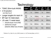
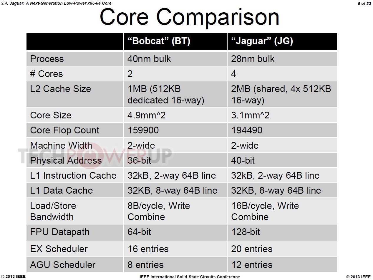
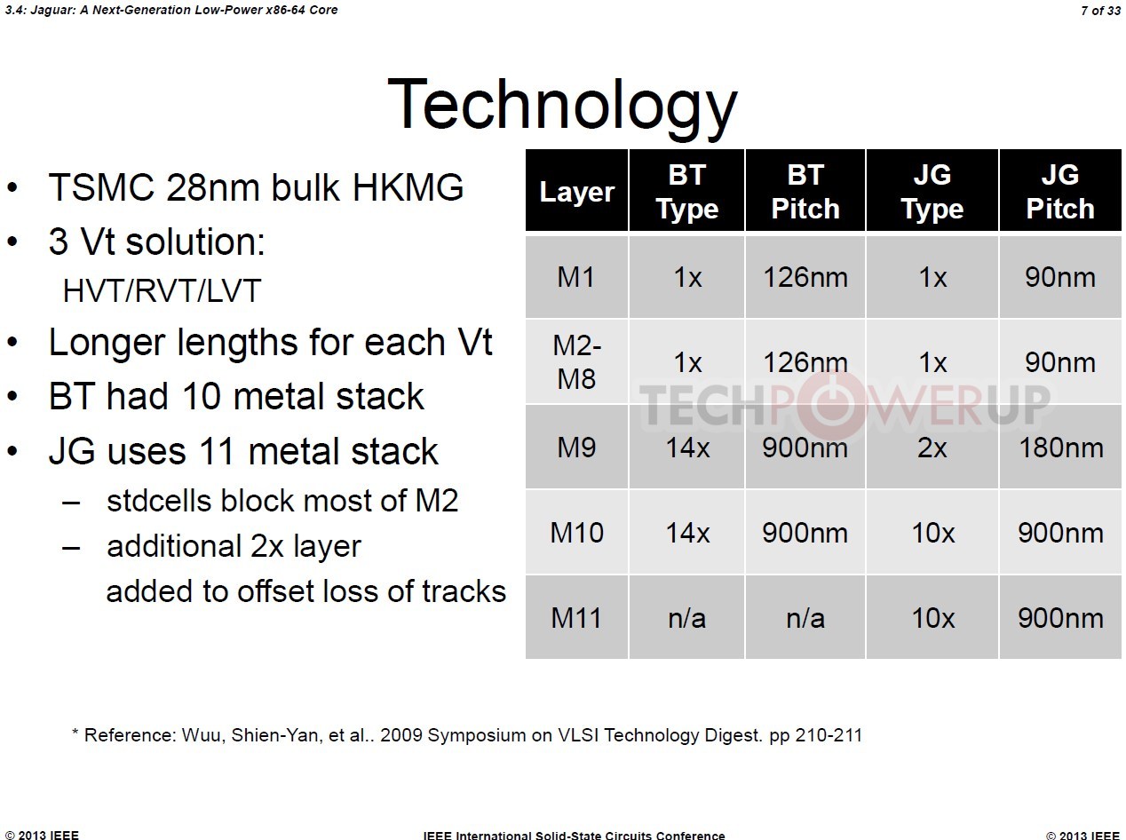
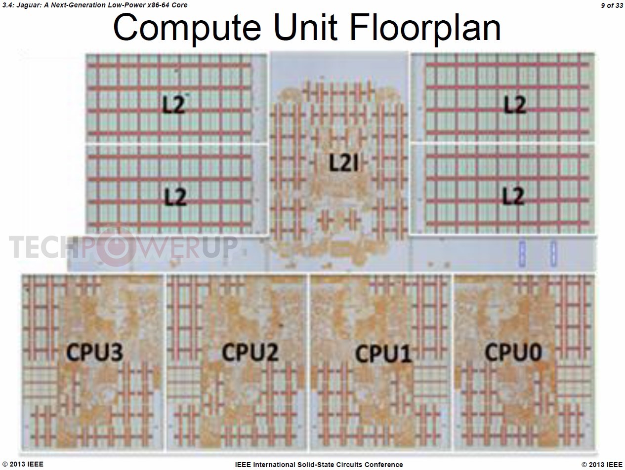
At its presentation at the 60th ISSC 2013 conference, AMD detailed "Jaguar," revealing a few killer features that could restore the company's competitiveness in the low-power CPU segment. To begin with, APUs with CPU cores based on this micro-architecture will be built on TSMC's 28-nanometer HKMG process. Jaguar allows for up to four x86-64 cores. The four cores, unlike Bulldozer modules, are completely independent, and only share a 2 MB L2 cache.
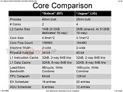
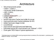
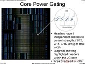
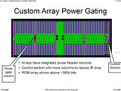
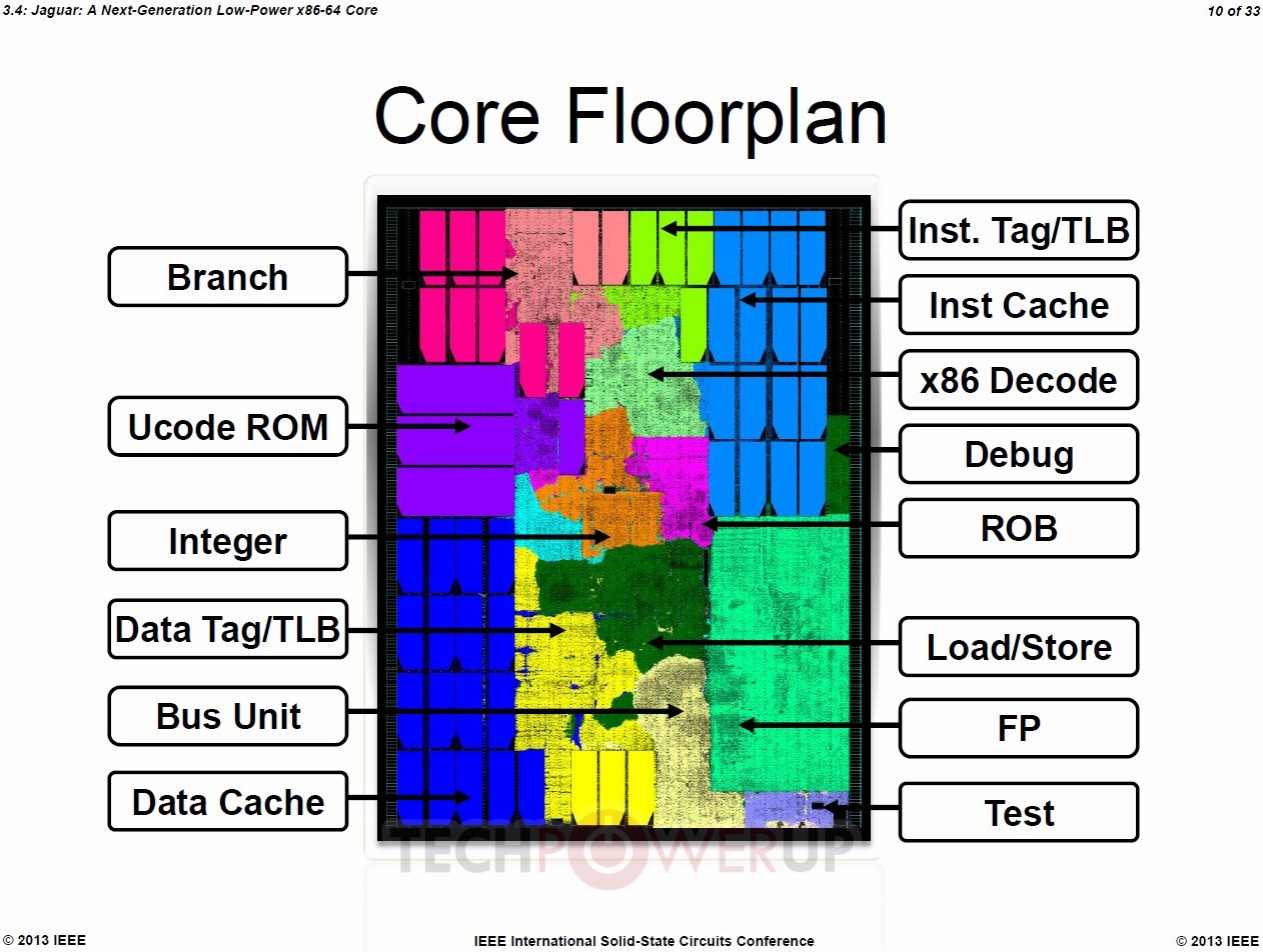
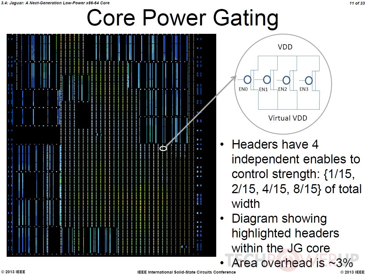
"Jaguar" x86-64 cores feature a 40-bit wide physical address (Bobcat features 36-bit), 16-byte/cycle load/store bandwidth, which is double that of Bobcat, a 128-bit wide FPU data-path, which again is double that of Bobcat, and about 50 percent bigger scheduler queues. The instruction set is where AMD is looking to rattle Atom. Not only does Jaguar feature out-of-order execution, but also ISA instruction sets found on mainstream CPUs, such as AVX (advanced vector extensions), SIMD instruction sets such as SSSE3, SSE4.1, SSE4.2, and SSE4A, all of which are quite widely adopted by modern media applications. Also added is AES-NI, which accelerates AES data encryption. In the efficiency department, AMD claims to have improved its power-gating technology that completely cuts power to inactive cores, to conserve battery life.
Add your own comment

71 Comments on AMD "Jaguar" Micro-architecture Takes the Fight to Atom with AVX, SSE4, Quad-Core

#26
Lionheart
Mussels[George Takei] Oh Myyyyyy [/Takei]


this should shake up the low end market a decent amount. intel atom is just too damn slow. aint nobody got time for it.
AGREED :cool:

Posted on Reply
#27
sergionography
McSteelWonder if it will go over 1.6 GHz, seeing how it's more efficient than the last generation, and uses 28nm process...
yes it will be clocked higher
btarunrAccording to AMD, it will be clocked up to 1.80 GHz.
no amd said it will be clocked 10% higher than what bobcat would've clocked at on 28nm node. that being said 1.8ghz is the worst case scenario, realistic scenario is probably about 20-30% higher due to the added stage in the pipleline in the design, and some due to the 28nm node, so 2ghz-2.2ghz is very likely, but seeing that they introduced a 25w tdp part on these i wont be surprise to see turbo clocks at over 2.4-2.8ghz(considering trinity 19w tdp parts do 2.0-2.8ghz)
xviI am SO glad to hear this.
yes but then bobcat/jaguar is half the bulldozer module, it has 2decoders and 128bit fpu vs bulldozers 4decoders and 256bit fpu ;)
Posted on Reply
#28
Aquinus
Resident Wat-man
sergionographyes but then bobcat/jaguar is half the bulldozer module, it has 2decoders and 128bit fpu vs bulldozers 4decoders and 256bit fpu
...and without any shared resources to run the additional thread like a module would. Most software can't utilize the 256-bit FPU yet anyways. So it's not like this is a gimped BD chip but rather it is a beefed up bobcat chip. There are a lot of CPU features and instructions that will be offered that is pretty neat.

Also you said something about the pipeline being larger. How do you figure? This CPU doesn't use modules or the module design so why would the pipeline be longer? Shouldn't it be similar to the PII pipeline?
Posted on Reply
#29
sergionography
Aquinus...and without any shared resources to run the additional thread like a module would. Most software can't utilize the 256-bit FPU yet anyways. So it's not like this is a gimped BD chip but rather it is a beefed up bobcat chip. There are a lot of CPU features and instructions that will be offered that is pretty neat.

Also you said something about the pipeline being larger. How do you figure? This CPU doesn't use modules or the module design so why would the pipeline be longer? Shouldn't it be similar to the PII pipeline?
yes but the bulldozer core can max out a big portion of the module on a single thread while a bobcat/jaguar cant use up a second core for better single thread ;) the fundamental behind the bulldozer is excellent, but the implementation was horrible, they shared way too much at once, and now with steamroller unsharing some of the parts like the decoder is proof for that, they shouldve started like jaguar, share the L2 cache, then go from there to share prefetch, and then other parts if needed

but now back to jaguar which is what this thread is about!
when jaguar was announced in the amd presentation they mentioned adding a stage to the pipleline, it used to be 11 now its 12 i believe, or 10 became 11 cant remember

and im talking about the integer pipelines, every cpu has one. and no pII had 13 stages if im not mistaken so bobcat had a new redesigned one. bulldozer has 19-22 also redesigned from pII
Posted on Reply
#30
Aquinus
Resident Wat-man
sergionographywhen jaguar was announced in the amd presentation they mentioned adding a stage to the pipleline, it used to be 11 now its 12 i believe, or 10 became 11 cant remember
Right, where did you read that because I can't find anything to confirm it.
Posted on Reply
#31
sergionography
AquinusRight, where did you read that because I can't find anything to confirm it.
semiaccurate goes briefly over the added stage in the pipeline and has an amd slide about it also, but what o remember for sure is a YouTube video i saw were they presented trinity and then jaguar, i will send links later as now im using my phone to reply
Posted on Reply
#32
ste2425
you got me all excited for nothing i though AMD was teaming up with jaguar for something then :(

AMD XJS
Posted on Reply
#33
lilhasselhoffer
An Atom style chip that doesn't suck. It's too bad that AMD didn't do this two years ago, and completely curb stomp Intel in the market.


As it stands, Intel is getting closer to making a viable Atom every revision. They suck on the graphics side, but have the weight to push Atom forward. AMD really caught the boat with an APU, but haven't done enough (as yet) to close the market to Intel offerings.


Here's to the hope that Intel will get thoroughly beaten by an excellent APU string. I'd get behind a quad core tablet running, ostensibly, 7xxx generation GCN graphics. It beats the tar out of the crap Intel has phoned in with Atom.
Posted on Reply
#35
sergionography
lilhasselhofferAn Atom style chip that doesn't suck. It's too bad that AMD didn't do this two years ago, and completely curb stomp Intel in the market.


As it stands, Intel is getting closer to making a viable Atom every revision. They suck on the graphics side, but have the weight to push Atom forward. AMD really caught the boat with an APU, but haven't done enough (as yet) to close the market to Intel offerings.


Here's to the hope that Intel will get thoroughly beaten by an excellent APU string. I'd get behind a quad core tablet running, ostensibly, 7xxx generation GCN graphics. It beats the tar out of the crap Intel has phoned in with Atom.
what are you talking about? bobcat stomped atom on so many levels
Posted on Reply
#36
AlB80
Ps4

I heard JG will be inside PS4.
ps. 1.6GHz
Posted on Reply
#37
NinkobEi
the PS4 will have an 8-core version @ 1.84 ghz. Or will it just be two Jaguars? A mommy and a poppy. Hmm. Anyone seen the benchies for this puppy yet?
Posted on Reply
#38
Ikaruga
NinkobEithe PS4 will have an 8-core version @ 1.84 ghz. Or will it just be two Jaguars? A mommy and a poppy. Hmm. Anyone seen the benchies for this puppy yet?
What we "know" so far about about Orbis's CPU (from the rumors/leaks) is this:

- Orbis contains eight Jaguar cores at 1.6 Ghz, arranged as two “clusters”
- Each cluster contains 4 cores and a shared 2MB L2 cache
- 256-bit SIMD operations, 128-bit SIMD ALU
- SSE up to SSE4, as well as Advanced Vector Extensions (AVX)
- One hardware thread per core
- Decodes, executes and retires at up to two intructions/cycle
- Out of order execution
- Per-core dedicated L1-I and L1-D cache (32Kb each)
- Two pipes per core yield 12,8 GFlops performance
- 102.4 GFlops for system

1.6Ghz might get a little boost before the release, since they also doubled the RAM from 4GB to 8GB already.

btw a little off-toppic: anyone has any idea, how the hell are they going to deal with the insane amount of latency of the GDDR5 as main memory, this is something which puzzles me since yesterday?
Posted on Reply
#39
cadaveca
My name is Dave
IkarugaWhat we "know" so far about about Orbis's CPU (from the rumors/leaks) is this:

- Orbis contains eight Jaguar cores at 1.6 Ghz, arranged as two “clusters”
- Each cluster contains 4 cores and a shared 2MB L2 cache
- 256-bit SIMD operations, 128-bit SIMD ALU
- SSE up to SSE4, as well as Advanced Vector Extensions (AVX)
- One hardware thread per core
- Decodes, executes and retires at up to two intructions/cycle
- Out of order execution
- Per-core dedicated L1-I and L1-D cache (32Kb each)
- Two pipes per core yield 12,8 GFlops performance
- 102.4 GFlops for system

1.6Ghz might get a little boost before the release, since they also doubled the RAM from 4GB to 8GB already.

btw a little off-toppic: anyone has any idea, how the hell are they going to deal with the insane amount of latency of the GDDR5 as main memory, this is something which puzzles me since yesterday?
What Latency?
Posted on Reply
#40
Aquinus
Resident Wat-man
Ikarugabtw a little off-toppic: anyone has any idea, how the hell are they going to deal with the insane amount of latency of the GDDR5 as main memory, this is something which puzzles me since yesterday?
cadavecaWhat Latency?
I don't think latency is going to be a problem. If they're using GDDR5 for main memory as well as video memory then I suspect that the CPU will directly access memory. It's not like a discrete GPU on a computer where you have to copy the data over the PCI-E bus where latency would be a very real issue, but I don't think that will be the case.
Posted on Reply
#41
sergionography
IkarugaWhat we "know" so far about about Orbis's CPU (from the rumors/leaks) is this:

- Orbis contains eight Jaguar cores at 1.6 Ghz, arranged as two “clusters”
- Each cluster contains 4 cores and a shared 2MB L2 cache
- 256-bit SIMD operations, 128-bit SIMD ALU
- SSE up to SSE4, as well as Advanced Vector Extensions (AVX)
- One hardware thread per core
- Decodes, executes and retires at up to two intructions/cycle
- Out of order execution
- Per-core dedicated L1-I and L1-D cache (32Kb each)
- Two pipes per core yield 12,8 GFlops performance
- 102.4 GFlops for system

1.6Ghz might get a little boost before the release, since they also doubled the RAM from 4GB to 8GB already.

btw a little off-toppic: anyone has any idea, how the hell are they going to deal with the insane amount of latency of the GDDR5 as main memory, this is something which puzzles me since yesterday?
we also know it will have 18gcn clusters = 1152 gcn cores rated at 800mhz
and it was rated at 1.84gflops or something actually

as for the latency then i guess its up to the custom hsa memory controller, i would bet on that to handle things, after all the chip is an apu and its interesting to see what a buff apu can do, as the latency between cpu and gpu is much lower so gpgpu on an apu is much better than on a dedicated gpu with the same specs, and with gddr5 the high bandwidth will cover up the latency especialy that on consoles developers will optimize specifically for the hardware so it wont be too hard to tap into the flops available

and above all the good news out of this is that amd is smart to offer a multicore solution with with high latency to optimize because if anything this will only make their desktop solutions shine in future games since developers will start to work around it. this might explain why with steamroller amd paid no attention to most of the higher level cache subsystem (high latency on l3 and l2 cache)
Posted on Reply
#42
AsRock
TPU addict
DannibusXI wouldn't have named my product anything close to the Atari Jaguar.
LMAO, for some odd reason it was the 1st thing i thought when i read AMD Jaguar for what must been coursed by that terrible console.
Posted on Reply
#43
Mussels
Freshwater Moderator
sounds like they're planning crossfired APU's. for media/2D use, drop back to single CPU + GPU, then for games that require it, ramp it up to 8 core/dual GPU.
Posted on Reply
#44
Ikaruga
sergionographywe also know it will have 18gcn clusters = 1152 gcn cores rated at 800mhz
and it was rated at 1.84gflops or something actually
yep, I forgot about those changes, thanks.
cadavecaWhat Latency?
sergionographywe also know it will have 18gcn clusters = 1152 gcn cores rated at 800mhz
and it was rated at 1.84gflops or something actually

as for the latency then i guess its up to the custom hsa memory controller, i would bet on that to handle things, after all the chip is an apu and its interesting to see what a buff apu can do, as the latency between cpu and gpu is much lower so gpgpu on an apu is much better than on a dedicated gpu with the same specs, and with gddr5 the high bandwidth will cover up the latency especialy that on consoles developers will optimize specifically for the hardware so it wont be too hard to tap into the flops available

and above all the good news out of this is that amd is smart to offer a multicore solution with with high latency to optimize because if anything this will only make their desktop solutions shine in future games since developers will start to work around it. this might explain why with steamroller amd paid no attention to most of the higher level cache subsystem (high latency on l3 and l2 cache)
Don't forget that it's not DDR5 but GDDR5! There is a significant difference. GDDR5 is basically a heavily tweaked DDR3 (well, not exactly, but let's just forgot the little details for the sake of the subject). They sacrifice the low latency of the DDR3 to boost the bandwidth. GPUs don't really need very low latencies since their parallel nature "comes to the rescue" when a thread/calculation stalls, and only internal speed what matters the most, to be able to move large amount of data chunks as fast as possible.

Don't get me wrong, I'm sure Sony knows what they are doing and eight CPU cores is apparently makes it parallel enough to use GDDR5 as system memory, but I'm still very curious how they are doing it, because if it's better, I sure want something like that on our PC side as well:toast:
Posted on Reply
#45
de.das.dude
Pro Indian Modder
this is good. way to go AMD. intel atom is seriously slow. even running windows 7 is a chore. aint nobody got time for that :laugh:
Posted on Reply
#46
Aquinus
Resident Wat-man
IkarugaDon't forget that it's not DDR5 but GDDR5! There is a significant difference. GDDR5 is basically a heavily tweaked DDR3 (well, not exactly, but let's just forgot the little details for the sake of the subject). They sacrifice the low latency of the DDR3 to get boost the bandwidth. GPUs don't really need very low latencies since their parallel nature "comes to the rescue" when a thread/calculation stalls, and only internal speed what matters the most, to be able to move large amount of data chunks sas fast as possible.
How do you figure? The actual timings might be higher but keep in mind that GDDR5 gets run at nutty high clock speeds. I think any issue with latency will be mitigated with proper pre-fetching and a large (and fast) CPU cache.
Posted on Reply
#47
Ikaruga
AquinusHow do you figure? The actual timings might be higher but keep in mind that GDDR5 gets run at nutty high clock speeds. I think any issue with latency will be mitigated with proper pre-fetching and a large (and fast) CPU cache.
It's probably the new 4Gb Hynix or Samsung chips available from Q1 this year (they gonna use 16 piece in clamshell mode I assume), and both of those will have 32ns latency, fairly high for any kind of CPU.... hence my technical curiosity.
Posted on Reply
#48
Aquinus
Resident Wat-man
IkarugaIt's probably the new 4Gb Hynix or Samsung chips available from Q1 this year (they gonna use 16 piece in clamshell mode I assume), and both of those will have 32ns latency, fairly high for any kind of CPU.... hence my technical curiosity.
What? You're joking right? The only CPUs out that are even capable of getting close to accessing memory in 32ns is an IVB chip. I couldn't even get close to that with my SB-E 3820. There are a lot of CPUs with more latency than that.

I think it will be fine. ;)

Posted on Reply
#49
Ikaruga
AquinusWhat? You're joking right? The only CPUs out that are even capable of getting close to accessing memory in 32ns is an IVB chip. I couldn't even get close to that with my SB-E 3820. There are a lot of CPUs with more latency than that.

I think it will be fine. ;)

www.techpowerup.com/forums/attachment.php?attachmentid=50174&stc=1&d=1361524743
No, and I don't really understand why would I joke about ram timings on my favorite enthusiast site. Do you understand that I was citing the actual latency of the chip itself, and not the latency the MC will have to deal with when accessing the memory?
For example, a typical DDR3@1600 module has about 12ns latency in a modern PC.
Posted on Reply
#50
McSteel
I believe that AIDA does round-trip latency, and Ikaruga (love that game btw) probably claims that the GDDR5 used has a CL of 32ns. 1600 MT/s CL9 DDR3 has a CL of ~11.25ns max, close to three times less.

Still, with some intelligent queues and cache management, this won't be too much of a problem.


## EDIT ##
Have I ever mentioned how I hate it when I get distracted when replying, only to find out I made myself look like an idiot by posting the exact same thing as the person before me? Well, I do.
Sorry Ikaruga.
Posted on Reply
Add your own comment
Jul 15th, 2024 20:54 EDT change timezone

New Forum Posts

Popular Reviews

Controversial News Posts