Thursday, September 26th 2013

Radeon R9 and Radeon R7 Graphics Cards Pictured Some More
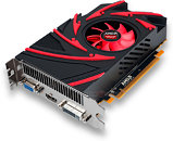
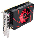
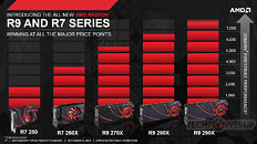
Here's a quick recap of AMD's updated product stack, spread between the R9 and R7 series. This article can help you understand the new nomenclature. AMD's lineup begins with the Radeon R7 250 and Radeon R7 260X. The two are based on the 28 nm "Curacao" silicon, which is a variation of the "Pitcairn" silicon the previous-generation Radeon HD 7870 was based on. The R7 250 is expected to be priced around US $89, with 1 GB of RAM, and performance rated at over 2,000 points by 3DMark Firestrike benchmark. The R7 260X, features double the memory at 2 GB, higher clock speeds, possibly more number crunching resources, Firestrike score of over 3,700 points, and a pricing that's around $139. This card should turn up the heat against the likes of GeForce GTX 650 Ti Boost.
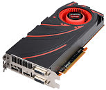
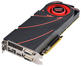
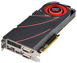
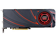
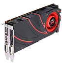
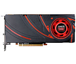
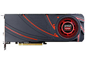
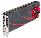
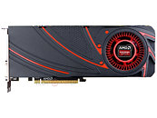
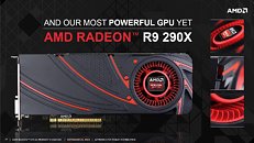
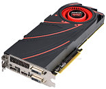
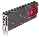
Moving on, there's the $199 Radeon R9 270X. Based on a chip not much unlike "Tahiti LE," it features 2 GB of memory, and 3DMark Firestrike score of over 5,500 points. Then there's the Radeon R9 280X. This card, priced attractively at $299, is practically a rebrand of the Radeon HD 7970 GHz Edition with. It features 3 GB of RAM, and over 6,800 points on 3DMark Firestrike. Then there are the R9 290 and R9 290X. AMD flew dozens of scribes thousands of miles over to Hawaii, and left them without an official announcement on the specifications of the two. From what AMD told us, the two feature 4 GB of memory, over 5,000 TFLOP/s compute power, and over 300 GB/s memory bandwidth. The cards we mentioned are pictured in that order below.More pictures follow.
Radeon R7 250Radeon R7 260XRadeon R9 270XRadeon R9 280XRadeon R9 290Radeon R9 290X





77 Comments on Radeon R9 and Radeon R7 Graphics Cards Pictured Some More
you are misguiding others with your myopic view of the world based on what most agree is a scant pr slide meant to churn the rumour mill.
but with you its allway's essentially,,
amd are lieing shit nobs ,OR they Are lieing shit nobs(cross out one or two from each side though each post) ,,, yeah your english makes it sound like more than that,, but it is'nt
Edit: this simplifies things a bit because they could reduce margins or design a new chip, but reducing margins would bring them back to the HD4000/GTX200 series price wars which are undesirable for them, and a redesigned low end chip would only be viable for a short time before 20nm came in and made it obsolete - they never would recoup their investment.
Someone with a brain. :respect:
If you go back and look at the presentation Raja when hes talking about "Over 5 TFLOPS Compute"
Hes talking about the series R9 290. Not specific to R9 290X.
GK110 - 780 to Titan there is a 517 differance
Tahiti - 7950 to 7970 GHZ there is a 1229 difference
Add that to the speculation...
7970 @ Stock (925/1375)
Fire Strike
Score:6622
Graphic Score:7402
7970 @ 7970 GHZ/Boost (1050/1500)
Fire Strike
Score:7210
Graphic Score:8235
Or is it verboten to speculate ? I seem to recall that many people here have speculated and hypothesised on much less information than that. Allow me to refresh your memory on your speculation for what is now called the 290X:As far as performance I speculated upon, I worked on the given information and came up with ~18% over the HD 7970GE based on the Firestrike slide with preliminary driver support, and and the FP32 numbers.The fact that the GTX 780 scores around the same:
Led me to conclude that the cards were likely evenly matched....as other sources have intimated:The other speculation I indulged in was price, and the GPU under the various cards skirts.
None of the speculation has been shown inordinately out of the likely expected parameters so far.
2816 Streaming Processors (2) (1000 MHz boost) = 5.632 GFLOPs.
If you consider the OC potential of the previous generations. The average is at around 30%,
Single 6990 base clock is 830 Mhz. It's max OC is roughly around 1060 to 1120 Mhz. 27.71%
Single 7970 base clock is 900 Mhz. 1050 Mhz boost. It's max OC is roughly 1321 Mhz w/ LN2. 46.78%
Single 7990 base clock is 950 Mhz. 1000 Mhz boost. It's max OC is roughly 1100 Mhz. 10.00%; this may actually be higher...
Average all together from up above = 28.16%...
What's my point.
10% OC headroom: 1.1 x 5.632 GFLOPs = 6.19852 GFLOPs.
20% OC headroom: 1.2 x 5.632 GFLOPs = 6.7584 GFLOPs.
28.16% OC Headroom: 1.2816 x 5.632 GFLOPs = 7.21813 GFLOPs.
30.00% OC Headroom: 1.3 x 5.632 GFLOPs = 7.3216 GFLOPs.
So, if plausible, it may not be that difficult or impossible to surpass the 5.0 to 6.0 GFLOPs boundaries with the up coming R9-990... Sadly, only time will tell...
As to what you bolded in my words you need to revival the context of the question:I believe I used W1zzard reference GTX780 review and that could've skewed the percentages a little.
www.techpowerup.com/reviews/NVIDIA/GeForce_GTX_780/26.html
All I was saying if they could deliver such performance (of a 7990), it would be much more than I could envision... I didn't say I was expecting. While I wrote Volcanic... meant what does that means for 20Nm process in a couple of month most still though Q1 '14, even in July it was thought Volcanic Island was 20Nm.
I exhaled a while back... take a breath and wait for the 15th. ;)
1) The few die-hards still using 1600/1920x1200 CRTs
2) Reviewers who test monitors for latency by comparing an LCD with a CRT.
Also i use a VGA monitor with my GTX 560 because of budget i couldn't get a new monitor. Just because people can get great hardware to go in the case doesn't mean they aren't stretching their limit. Hell i don't plan to replace my current monitor until it breaks so i may be part of that voiceless userbase ;) lol
VGA has a resolution limitation of about 3MP (QXGA 2048x1536) @60Hz; if you are using a VGA monitor, you can't have a resolution above that, but even those types of monitors are rare. These high end cards are overkill for a single 2MP or 3MP 60Hz monitor. Rest assured, the mid range and lower end cards have DVI-I ports so that you can still use cheap VGA adapters, and they are a much better performance match for the VGA resolutions.
EDIT: Interestingly enough, DisplayPort to VGA adapters are much cheaper than DVI-D to VGA adapters. You can get a DisplayPort to VGA adapter for $24.71, although it is limited to 1920x1200 @60Hz (not QXGA 2048x1536 @60Hz).