Sunday, February 8th 2015

Radeon R9 380X Based on "Grenada," a Refined "Hawaii"
AMD's upcoming Radeon R9 380X and R9 380 graphics cards, with which it wants to immediately address the GTX 980 and GTX 970, will be based on a "new" silicon codenamed "Grenada." Built on the 28 nm silicon fab process, Grenada will be a refined variant of "Hawaii," much in the same way as "Curacao" was of "Pitcairn," in the previous generation.
The Grenada silicon will have the same specs as Hawaii - 2,816 GCN stream processors, 176 TMUs, 64 ROPs, and a 512-bit wide GDDR5 memory interface, holding 4 GB memory. Refinements in the silicon over Hawaii could allow AMD to increase clock speeds, to outperform the GTX 980 and GTX 970. We don't expect the chip to be any more energy efficient at its final clocks, than Hawaii. AMD's design focus appears to be performance. AMD could save itself the embarrassment of a loud reference design cooler, by throwing the chip up for quiet custom-design cooling solutions from AIB (add-in board) partners from day-one.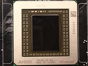 In other news, the "Tonga" silicon, which made its debut with the performance-segment Radeon R9 285, could form the foundation of Radeon R9 370 series, consisting of the R9 370X, and the R9 370. Tonga physically features 2,048 stream processors based on the more advanced GCN 1.3 architecture, 128 TMUs, 32 ROPs, and a 384-bit wide GDDR5 memory interface. Both the R9 370 and R9 370X could feature 3 GB of standard memory amount.
The only truly new silicon with the R9 300 series, is "Fiji." This chip will be designed to drive AMD's high-end single- and dual-GPU graphics cards, and will be built to compete with the GM200 silicon from NVIDIA, and the GeForce GTX TITAN-X it will debut with. This chip features 4,096 stream processors based on the GCN 1.3 architecture - double that of "Tonga," 256 TMUs, 128 ROPs, and a 1024-bit wide HBM memory interface, offering 640 GB/s of memory bandwidth. 4 GB could be the standard memory amount. The three cards AMD will carve out of this silicon, are the R9 390, the R9 390X, and the R9 390X2.
Source:
3DCenter.org
The Grenada silicon will have the same specs as Hawaii - 2,816 GCN stream processors, 176 TMUs, 64 ROPs, and a 512-bit wide GDDR5 memory interface, holding 4 GB memory. Refinements in the silicon over Hawaii could allow AMD to increase clock speeds, to outperform the GTX 980 and GTX 970. We don't expect the chip to be any more energy efficient at its final clocks, than Hawaii. AMD's design focus appears to be performance. AMD could save itself the embarrassment of a loud reference design cooler, by throwing the chip up for quiet custom-design cooling solutions from AIB (add-in board) partners from day-one.

The only truly new silicon with the R9 300 series, is "Fiji." This chip will be designed to drive AMD's high-end single- and dual-GPU graphics cards, and will be built to compete with the GM200 silicon from NVIDIA, and the GeForce GTX TITAN-X it will debut with. This chip features 4,096 stream processors based on the GCN 1.3 architecture - double that of "Tonga," 256 TMUs, 128 ROPs, and a 1024-bit wide HBM memory interface, offering 640 GB/s of memory bandwidth. 4 GB could be the standard memory amount. The three cards AMD will carve out of this silicon, are the R9 390, the R9 390X, and the R9 390X2.
156 Comments on Radeon R9 380X Based on "Grenada," a Refined "Hawaii"
All I'm saying is that it's a selling point and nothing bad comes out of improving efficiency.
Now show me a single monitor difference? Something large majority of users have...
I've been reading some rumors that say the R9 380X will be more power efficient and with the same number of cores as the R9 290X and more room to push the clocks higher due to improved efficiency then it should take the title from Nvidia as the fastest GPU around.
Right about HBM...plus, if they shrink/reconfigure the core design on 14/16nm for 50% more resources, the mem controller could probably be reasonably recycled....it's also possible they could cut cache or what-not because of that off-die bw. Not saying they did/will...but who knows? It's possible it's there for more than being ahead-of-it's-time (but a necessary evil) on bw and behind-it's-time on density configuration. Even if they didn't change anything, it should be good for a good extra chunk of performance (double over what is required gives typically around a 16% boost...this in essence could give something like 8% over what one might expect given the other specs and typical core usage).
Either way you look at it, this thing *has* to compete with a GM200 21SMM part. Say that can do 1400mhz best-case, that essentially means this has to do 1200 to compete. The bandwidth required for quite literally 10TF is..well...a lot. You'd be talking needing an 8ghz/512-bit controller which wouldn't exactly be small nor power efficient (if even possible with within die size limits). As odd as it sounds, twice the controllers at (what apparently amounts to 5ghz) is likely both less transistors and more efficient within the gpu logic..Correct. HBM is currently 1GB. Implementation, unlike the setup of gddr5, is limited to four chips. That means 4GB. 2nd gen is due end of year. Does that mean a refresh before 14/16nm? Conceivably...but who knows how fast amd is transitioning to the smaller process. I continue to disagree about 4GB being enough...If one was to argue things should be properly coded for 4k/8GB (or possibly 6GB in many instances), we could have a conversation. That said, it's not going to stop HBM memory density from increasing and badly optimized console ports targeted toward that shared pool of memory at a low resolution from being a scaling factor in some regards. I still stand by GM200/R390x for the most part being 1440p-targeted chips (think in terms of a 900p 30fps ps4 game scaled to 1440p/60)...just like GM204 is mostly a 1080p-targeted chip. In those respects, it can be argued 4GB(/6GB in some cases) is sufficient.
Cannot wait to see more of the develop!
In short r9-380/x, r9-370/x and r7-260/x(I really hope this isn't rebranded pitcairn as 3dcenter rumored it to be) is kind of meh been there done that. Really interesting parts will be r9-390 -series.
Also, yes, stacked memory needs some time to ramp up but I guess they needed to start at some point and it is now.
R9 290X Reference Card 17 watts
R9 290X Lightning 22 watts
GTX 980 Reference 8 watts
GTX 980 Gaming 14 watts
If leave your computer on 24 hours a day every day idling and you pay the national average per kWh (12 cents) then the reference R9 290X will add 78 cents a month to your power bill. For the factory OC cards the R9 290X will add 70 cents a month. It's just not much at all and if that amount matters to you or you pay a lot more for electricity then I would say turn your rig off when not in use.
goodpoint bro, just wait R300 and we can talk and compare it to G9 series, but if AMD too late, it'll another story..
Idling is not an issue. People are grasping at straws...
#4Kapable
Just saying.
You know fine well what I meant.