Sunday, February 8th 2015

Radeon R9 380X Based on "Grenada," a Refined "Hawaii"
AMD's upcoming Radeon R9 380X and R9 380 graphics cards, with which it wants to immediately address the GTX 980 and GTX 970, will be based on a "new" silicon codenamed "Grenada." Built on the 28 nm silicon fab process, Grenada will be a refined variant of "Hawaii," much in the same way as "Curacao" was of "Pitcairn," in the previous generation.
The Grenada silicon will have the same specs as Hawaii - 2,816 GCN stream processors, 176 TMUs, 64 ROPs, and a 512-bit wide GDDR5 memory interface, holding 4 GB memory. Refinements in the silicon over Hawaii could allow AMD to increase clock speeds, to outperform the GTX 980 and GTX 970. We don't expect the chip to be any more energy efficient at its final clocks, than Hawaii. AMD's design focus appears to be performance. AMD could save itself the embarrassment of a loud reference design cooler, by throwing the chip up for quiet custom-design cooling solutions from AIB (add-in board) partners from day-one.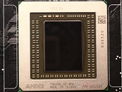 In other news, the "Tonga" silicon, which made its debut with the performance-segment Radeon R9 285, could form the foundation of Radeon R9 370 series, consisting of the R9 370X, and the R9 370. Tonga physically features 2,048 stream processors based on the more advanced GCN 1.3 architecture, 128 TMUs, 32 ROPs, and a 384-bit wide GDDR5 memory interface. Both the R9 370 and R9 370X could feature 3 GB of standard memory amount.
The only truly new silicon with the R9 300 series, is "Fiji." This chip will be designed to drive AMD's high-end single- and dual-GPU graphics cards, and will be built to compete with the GM200 silicon from NVIDIA, and the GeForce GTX TITAN-X it will debut with. This chip features 4,096 stream processors based on the GCN 1.3 architecture - double that of "Tonga," 256 TMUs, 128 ROPs, and a 1024-bit wide HBM memory interface, offering 640 GB/s of memory bandwidth. 4 GB could be the standard memory amount. The three cards AMD will carve out of this silicon, are the R9 390, the R9 390X, and the R9 390X2.
Source:
3DCenter.org
The Grenada silicon will have the same specs as Hawaii - 2,816 GCN stream processors, 176 TMUs, 64 ROPs, and a 512-bit wide GDDR5 memory interface, holding 4 GB memory. Refinements in the silicon over Hawaii could allow AMD to increase clock speeds, to outperform the GTX 980 and GTX 970. We don't expect the chip to be any more energy efficient at its final clocks, than Hawaii. AMD's design focus appears to be performance. AMD could save itself the embarrassment of a loud reference design cooler, by throwing the chip up for quiet custom-design cooling solutions from AIB (add-in board) partners from day-one.

The only truly new silicon with the R9 300 series, is "Fiji." This chip will be designed to drive AMD's high-end single- and dual-GPU graphics cards, and will be built to compete with the GM200 silicon from NVIDIA, and the GeForce GTX TITAN-X it will debut with. This chip features 4,096 stream processors based on the GCN 1.3 architecture - double that of "Tonga," 256 TMUs, 128 ROPs, and a 1024-bit wide HBM memory interface, offering 640 GB/s of memory bandwidth. 4 GB could be the standard memory amount. The three cards AMD will carve out of this silicon, are the R9 390, the R9 390X, and the R9 390X2.
156 Comments on Radeon R9 380X Based on "Grenada," a Refined "Hawaii"
Was Havok 2.0 not coming with massive improvements?
PhysX as is is just a joke, mainly because no one should bother with it on any serious level if only Nvidia users can make use of it.
All it is is gimmicky effects here and there, some smoke moving in batman, some flying orbs in borderlands or warframe, whoopdishit yo.
I am done with this thread, turning in an AMD fanboy thread trying to twist history to make AMD look like the super hero with a can do no wrong persona and Nvidia the super villain.
Anyway, bring on the low/mid level I say! That's where the REAL action is!
Once the words "rebrand" and "PhysX" got posted it was light the blue touch paper and cue the Mission Impossible theme.
Not that it matters much nowadays (can't recall any recent Physx game except for the Batmans) but I resented nVidia a lot back in the day... more so considering that I was one of the suckers that bought the Ageia card back then and nVidia threw us under a bus as soon as they bought them.
/rant
I'm guessing 390 will go for $400 and 390X will go for $500 or more. If those prices are $100 cheaper than that guesstimate, it'll be a tough choice for me to pick between the two.
Many will be simply skipping anything on this pesky 28 nm process. :(
R.I.P thread! :D
If you guys have a problem with certain people making fanboy comments, ignore the person and move on already otherwise you just make them feel important while they cook up excuses/retorts and that you care which in turn ruins threads.
Back to the topic at hand, the disappointment for this announcement only to me is that the R9 380X is not going to be the next big part/a new part. Though I guess depending on how well they improve/refine Hawaii into Grenada we might see something truly impressive. Though the real chip everyone has their eyes on is the R9 390X and what it brings to the table.
Then of course depending which tmsc manufacturing node they are using, moving to more effiency 28nm node might improve energy consumption(I think nvidia uses 28nm hpc for gm204/gm206 and amd uses 28nm hp? not the same node anyway). So can Grenada based r9-380-series be faster than gtx980/970 sure, but better perf/W very unlikely.
By the way, we are still paying pretty much the same price for quad core CPUs, and that is absolutely pathetic. The manufacturing costs must be insanely low.
2009 Lynnfield 45 nm 290 mm2 - 196 $
2014 Haswell 22 nm 177 mm2 - 182 $ (242 $ for a model that allows overclocking, sick)
We should have had six-core CPUs for 200 $ by now.
Die size is not a problem for GPUs. High-end GPUs are usually between 400 and 600 mm2, so heat dissipation is not a problem.
Whenever they change the node, they pack a lot more transistors into the chips, making them much faster while keeping a similar die size. Intel do not do that anymore, they are reducing the die size without increasing performance or clock speeds.
is it possible they cant fit anymore transistors since its smaller?
where would I look for some more inside info on chip engineering?
By the way.... you can counter this trend simply by ignoring the existence of Intel.
Just be smarter and buy all AMD. ;)
I miss the days where AMD CPUs were better for gaming (Duron, Athlon XP, Athlon 64), while being cheaper as well.
At least the GPUs are ok, though power hungry, but they are not really AMD, they just bought what was good.