Thursday, June 16th 2016

AMD "Ellesmere" ASIC Pictured Up Close in RX 480 PCB Picture Leak

AMD's all-important Polaris10 "Ellesmere" ASIC is pictured up close in a 3-quarter PCB shot of the upcoming Radeon RX 480 / RX 470. The picture reveals the ASIC with a die that's significantly smaller than that of the 28 nm "Tonga" silicon. The "Ellesmere" die is built on the 14 nm FinFET+ process. The die is seated on a substrate with a 256-bit wide GDDR5 memory interface. This appears to be a common reference PCB between the RX 480 and the RX 470.

The RX 480 ships with a classy looking lateral-flow cooler that's longer than the PCB itself; while the RX 470 uses a more common fin-stack top-flow cooling solution. Of course both cards are expected to ship with custom-design boards and cooling solutions. The reference PCB draws power from a single 6-pin PCIe power connector, and uses a 6-phase VRM to condition it for the GPU and memory. Display outputs include three DisplayPort 1.4 and one HDMI 2.0a connectors. There are also unused traces on the PCB for a DVI connector, so it's likely that some custom-design cards could feature it.
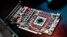
Source: VideoCardz
Add your own comment

73 Comments on AMD "Ellesmere" ASIC Pictured Up Close in RX 480 PCB Picture Leak

#51
medi01
"Naked" 480, not sure why it is a thing, but here we go:


@cdawall
Why do you think it would be "Fury replacement"? (at stock)
I could see 300$ (1500+) version going there, but don't 1266Mhz leaks show it somewhere at 980 (stock), and even slightly below it?
Posted on Reply
#52
A guy who knows things.
medi01"Naked" 480, not sure why it is a thing, but here we go:


@cdawall
Why do you think it would be "Fury replacement"? (at stock)
I could see 300$ (1500+) version going there, but don't 1266Mhz leaks show it somewhere at 980 (stock), and even slightly below it?
36 CU's says it all.

This card is an R9 390 replacement at a better price.

Vega will bring the Fury replacement cards. Only these will be called the RX 490/x this time.

I don't expect much better performance than the R9 390 if both cards are clocked the same in DX11 titles. This card will sit firmly in the R9 390x performance range but it's clockspeeds will help it pull away in some games.
Posted on Reply
#53
cdawall
where the hell are my stars
medi01@cdawall
Why do you think it would be "Fury replacement"? (at stock)
I could see 300$ (1500+) version going there, but don't 1266Mhz leaks show it somewhere at 980 (stock), and even slightly below it?
When did I say it replaced a fury? It should compete with a nano on the top end, but they will both be power limited minus the high end ones I feel.
Posted on Reply
#54
Mussels
Freshwater Moderator
from everything i've seen its a 390(x) replacement at half the TDP.

odd/annoying that the cooler is longer than the PCB.
Posted on Reply
#55
Slizzo
Musselsfrom everything i've seen its a 390(x) replacement at half the TDP.

odd/annoying that the cooler is longer than the PCB.
Fury is the exact same way though.
Posted on Reply
#56
sergionography
cdawallYou missed the entire point of my post. Clockspeed doesn't matter. GPU's do not have cores you are correct, but do you know what an SP is, do you know how they work? Did you know they stuff as many of those into a GPU as is possible and those basically make the GPU. Something about number of transistors and those actually do the work.

So instead of arguing with the entire forum, all of whom has said you are wrong how about do some research.

Oh and just in case you missed it clockspeed doesn't matter. The GTX980 hit 2.3ghz in 2015, it also wasn't the first GPU to do so. www.kitguru.net/components/graphic-cards/anton-shilov/evga-geforce-gtx-980-hits-2-30ghz-sets-new-records/
Lol ok I feel like you arent even reading my comments, or maybe you are slightly skipping through the lines. This time i will try to break things down as much as possible. There are 3 major factors in gpu production.
1- thermal headroom (dictates form factor)
2-die size (effects cost of production)
3- performance (number of cores/sps and clockspeed dictate this)

So in a gpu, engineers want to design power efficient sps to cram as many of them before reaching thermal headroom, but at the same time you want to clock them as high as you can as well in order to build reasonably priced/smaller chips that perform well. So there is always a trade off.

The question i presented here, is wether you believe clockspeed is a design decision by Amd, or is due to the variance between 14nm glofo and 16nm tsmc, id appreciate it if you stop refuting what you are assuming im trying to say(bash amd, which I'm not) and instead contribute to the conversation by answering my question.

Is amd prioratizing core count and bigger die with lower power over smaller chips with higher clocks and higher power?
And i also pointed out that I wonder if 14nm glofo having slightly higher density and possibly lower cost effected that decision from AMDs side.

Again sorry for the confusion, but you guys seriously didnt get what i was trying to say initially, but i hope you do now :)
Posted on Reply
#57
cdawall
where the hell are my stars
sergionographyLol ok I feel like you arent even reading my comments, or maybe you are slightly skipping through the lines. This time i will try to break things down as much as possible. There are 3 major factors in gpu production.
1- thermal headroom (dictates form factor)
2-die size (effects cost of production)
3- performance (number of cores/sps and clockspeed dictate this)

So in a gpu, engineers want to design power efficient sps to cram as many of them before reaching thermal headroom, but at the same time you want to clock them as high as you can as well in order to build reasonably priced/smaller chips that perform well. So there is always a trade off.

The question i presented here, is wether you believe clockspeed is a design decision by Amd, or is due to the variance between 14nm glofo and 16nm tsmc, id appreciate it if you stop refuting what you are assuming im trying to say(bash amd, which I'm not) and instead contribute to the conversation by answering my question.

Is amd prioratizing core count and bigger die with lower power over smaller chips with higher clocks and higher power?
And i also pointed out that I wonder if 14nm glofo having slightly higher density and possibly lower cost effected that decision from AMDs side.

Again sorry for the confusion, but you guys seriously didnt get what i was trying to say initially, but i hope you do now :)
What you have said is wrong. Claiming efficiency purely based off of clockspeed is ignorant. This tangent about sp's has never been in any of your comments and your understanding of it makes me think you watched one too many YouTube videos. Go back to Tom's hardware.
Posted on Reply
#58
Mussels
Freshwater Moderator
sergio: you're comparing apples to oranges and arguing over which is better because it has more blue.

clockspeed alone means nothing, you cannot use it as a reference between different models of the same GPU, let alone different GPU designs.
Posted on Reply
#59
sergionography
cdawallWhat you have said is wrong. Claiming efficiency purely based off of clockspeed is ignorant. This tangent about sp's has never been in any of your comments and your understanding of it makes me think you watched one too many YouTube videos. Go back to Tom's hardware.
Because previously i used the generic term cores rather than sp's. i only pointed out clock speed and that nvidia went mad on the clocks, i assumed people here would get what i meant, instead it seems people including yourself are butthurt, and even after saying sorry for the misunderstanding and explaining in details what i was going for you still wanna go on and on about technicalities and what i said and what i didnt say rather than moving on and having a mature conversation.
Posted on Reply
#60
medi01
sergionographyAnd i also pointed out that I wonder if 14nm glofo having slightly higher density and possibly lower cost effected that decision from AMDs side.
Note that AMD crammed in more transistors into the same die area than Nvidia even when on the same node.
More things at lower clock or less at higher clocks is a design decision, with neither way being clearly "superior".

If RX 480 OCing rumors are true, AMD has clearly "first chips released" round, with 15-20%-ish boost from OC, vs 10-14%-ish from nVidia.
Posted on Reply
#61
sergionography
medi01Note that AMD crammed in more transistors into the same die area than Nvidia even when on the same node.
More things at lower clock or less at higher clocks is a design decision, with neither way being clearly "superior".

If RX 480 OCing rumors are true, AMD has clearly "first chips released" round, with 15-20%-ish boost from OC, vs 10-14%-ish from nVidia.
Yeah that makes sense, and having more oc headroom is good and was clear from your original post, but idk if its just me but i still feel like amd is clocking these chips conservatively even with the density vs clocks thing you mentioned, probably to make validation possible on a higher number of chips, but on later revisions snd probably rebrands im sure the clock will be much higher and somewhat closer to the clocks nvidia is reaching. We saw this with the hd7970 when it was released at 925mhz, then a ghz edition at 1050mhz was released on the next revision. One thing i know for sure though, i cant wait for the official reviews! If my educated guesses and assumptions are in their place, i suspect polaris 10 at its mid/end of its lifecycle and rebrands will be clocked and perform similar or close to gtx1070, but initially with current clocks and somewhat early silicon it wont come as close
Posted on Reply
#62
cdawall
where the hell are my stars
sergionographyBecause previously i used the generic term cores rather than sp's. i only pointed out clock speed and that nvidia went mad on the clocks, i assumed people here would get what i meant, instead it seems people including yourself are butthurt, and even after saying sorry for the misunderstanding and explaining in details what i was going for you still wanna go on and on about technicalities and what i said and what i didnt say rather than moving on and having a mature conversation.
No one is butt hurt everyone is scratching their collective heads trying to figure out why you think the ocean is full of soda.
Posted on Reply
#63
deemon
the54thvoidWhy are you so illogical? He said top spot. With no reference to anything else. Top spot. Not middle top. Bottom top. Top.

Sooooooooooooooooooo yeah.

Maybe Radeon Pro would be Top Spot but with occasional profile absences, the average would possibly drag it below GTX 1080.
top spot at populatiry, like GTX 970 is right now (which isn't the king of performance either... just most popular; best seller). store.steampowered.com/hwsurvey
Posted on Reply
#64
Aquinus
Resident Wat-man
I think there is some confusion about how GPUs work, so maybe a little bit of explanation is in order because everyone is acting like the number of shaders are the things that can do independent computations and this is not a true statement. Both nVidia and AMD have terms for what constitutes a full "core". For nVidia that's a "Streaming Multiprocessor" or SM and for AMD it's a "Compute Unit" or CU. Each CU/SM has all of the inner workings to do independent calculations however, it's usually these units that dispatch more fine-grained computations. So, for regular CPUs, it's just having cores inside of a package. For GPUs, it's like having very simple cores which are put inside more CPU-like complex cores, which are then put into the package.

Just like regular CPUs, there is a limit to how much parallel work can be accomplished on a GPU. There is an argument that could be made that despite similar shader counts, the fact that nVidia used fewer SMs clocked higher yielded a better benefit than more CUs clocked lower (also with fewer shaders per CU.)

So with that said, I think there is a lot more that goes into this than clock speed, or even hardware for that matter. How the drivers and applications dispatch any instructions to the GPU has just as much to do with it as the way the hardware is setup... but simply put, the only time you can boil everything down to clock speed is on the same architecture.

tl;dr: GPUs do have "cores", they're just a little different than traditional CPU cores and they're not the shaders though, they're the CUs and SMs.
Posted on Reply
#65
Caring1
medi01"Naked" 480, not sure why it is a thing, but here we go:

Just wondering, the picture shows the fins on the heatsink in a vertical alignment, but shouldn't they mount 90 degrees to that for air flow to have a clean path out the rear vents?
Posted on Reply
#66
Mussels
Freshwater Moderator
to me, based on the base of that heatsink it needs to be rotated 90 degrees to the right - then the fins are horizontal, and it looks like it all lines up.
Posted on Reply
#67
Caring1
Musselsto me, based on the base of that heatsink it needs to be rotated 90 degrees to the right - then the fins are horizontal, and it looks like it all lines up.
That's what I thought, but the mounting holes look like they wont line up that way.
Maybe that is an illusion.
Posted on Reply
#68
sergionography
AquinusI think there is some confusion about how GPUs work, so maybe a little bit of explanation is in order because everyone is acting like the number of shaders are the things that can do independent computations and this is not a true statement. Both nVidia and AMD have terms for what constitutes a full "core". For nVidia that's a "Streaming Multiprocessor" or SM and for AMD it's a "Compute Unit" or CU. Each CU/SM has all of the inner workings to do independent calculations however, it's usually these units that dispatch more fine-grained computations. So, for regular CPUs, it's just having cores inside of a package. For GPUs, it's like having very simple cores which are put inside more CPU-like complex cores, which are then put into the package.

Just like regular CPUs, there is a limit to how much parallel work can be accomplished on a GPU. There is an argument that could be made that despite similar shader counts, the fact that nVidia used fewer SMs clocked higher yielded a better benefit than more CUs clocked lower (also with fewer shaders per CU.)

So with that said, I think there is a lot more that goes into this than clock speed, or even hardware for that matter. How the drivers and applications dispatch any instructions to the GPU has just as much to do with it as the way the hardware is setup... but simply put, the only time you can boil everything down to clock speed is on the same architecture.

tl;dr: GPUs do have "cores", they're just a little different than traditional CPU cores and they're not the shaders though, they're the CUs and SMs.
Well said, i personally didnt intend to get into sucj depth though and just used the term "cores" whereas in a cpu it was a handful while in a gpu its multi parallelism, and what i was saying the relationships between clockspeed to performance isnt the same as in cpus because in a cpu single core performance is key. In a gpu as i mentioned the big constrain is thermal headroom and die size, and you want to keep a good balance hence why i had all these question marks and everyone lost it. I said nvidia went mad on clocks and they surely did, yes you cant compare clockspeed directly between different architectures but i mean this is an over 30% clock difference between amd and nvidia, and this is kinda on similar nodes, so idk if im missing something but i dont remember the clockspeed gap ever being this wide to be honest, correct me if im wrong tho. I did point out 14nm vs 16nm so technicaly this is the first time amd and nvidia use different processes, still i though they should be similar for the most part
Posted on Reply
#69
cdawall
where the hell are my stars
sergionographyWell said, i personally didnt intend to get into sucj depth though and just used the term "cores" whereas in a cpu it was a handful while in a gpu its multi parallelism, and what i was saying the relationships between clockspeed to performance isnt the same as in cpus because in a cpu single core performance is key. In a gpu as i mentioned the big constrain is thermal headroom and die size, and you want to keep a good balance hence why i had all these question marks and everyone lost it. I said nvidia went mad on clocks and they surely did, yes you cant compare clockspeed directly between different architectures but i mean this is an over 30% clock difference between amd and nvidia, and this is kinda on similar nodes, so idk if im missing something but i dont remember the clockspeed gap ever being this wide to be honest, correct me if im wrong tho. I did point out 14nm vs 16nm so technicaly this is the first time amd and nvidia use different processes, still i though they should be similar for the most part
They aren't similar in anyway. Just because two companies use 65nm or 14/16nm doesn't mean anything is the same internally....
Posted on Reply
#70
Aquinus
Resident Wat-man
cdawallThey aren't similar in anyway. Just because two companies use 65nm or 14/16nm doesn't mean anything is the same internally....
They're a lot more similar than you think. Sure, there may be some implementation differences but when push comes to shove, they're doing it the same way. When push comes to shove, it really comes down to nVidia opting for lower latency and low parallel throughput compared to AMD which opts for higher overall latency but, more parallel throughput. The amount of performance increasing clocks for any given design will almost always result in performance improvements however, increasing the width of the engine (such as increasing the number of shaders/SMs/CUs,) has limited benefit depending on the workload and how that workload was dispatched.

Either way, all of this is besides the point. I don't think anyone really understands what @sergionography is trying to say and all I'm saying is this:
Musselssergio: you're comparing apples to oranges and arguing over which is better because it has more blue.

clockspeed alone means nothing, you cannot use it as a reference between different models of the same GPU, let alone different GPU designs.
Posted on Reply
#71
cdawall
where the hell are my stars
AquinusThey're a lot more similar than you think. Sure, there may be some implementation differences but when push comes to shove, they're doing it the same way. When push comes to shove, it really comes down to nVidia opting for lower latency and low parallel throughput compared to AMD which opts for higher overall latency but, more parallel throughput. The amount of performance increasing clocks for any given design will almost always result in performance improvements however, increasing the width of the engine (such as increasing the number of shaders/SMs/CUs,) has limited benefit depending on the workload and how that workload was dispatched.

Either way, all of this is besides the point. I don't think anyone really understands what @sergionography is trying to say and all I'm saying is this:
Same argument could be made with AMD vs intel CPU's...AMD uses a different everything for everything.

Oh well at the end of the day I just got a 980Ti for my PC at work so I am going to enjoy that


Lol because I so need a 980Ti to run web browsers.
Posted on Reply
#72
BiggieShady
AquinusThe amount of performance increasing clocks for any given design will almost always result in performance improvements however, increasing the width of the engine (such as increasing the number of shaders/SMs/CUs,) has limited benefit depending on the workload and how that workload was dispatched.
You don't need that "almost" at all, unless you mean increasing the clocks beyond stability ... increasing parallelism in hardware must be harnessed by equally parallelized software, luckily all graphics processing is very SIMD parallelized by definition (same shader code being run for many pixels and vertices) ... so higher clocks and more throughput are both valid strategies and both are used - so far AMD and Nvidia are finding a sweet spot power efficiency wise for what they think gaming workload will consist of in next year or so (balancing fill rate vs. compute/shading and raw throughput vs. caching in their architectures)
Posted on Reply
#73
MikeX
I bet somebody will overclock/overvolt RX480 to near 50%, that will par with 1070 easily. Looking at the performance graph and clock speed, I'm sure it can be done.
Posted on Reply
Add your own comment
Aug 24th, 2024 15:08 EDT change timezone

New Forum Posts

Popular Reviews

Controversial News Posts