News Posts matching #Ellesmere

Return to Keyword Browsing

AMD Announces the Radeon RX 500 Series

AMD today announced the Radeon RX 500 series graphics cards. The lineup is based on a "refined" variants of the "Polaris" family of GPUs that power the RX 400 series. These include manufacturing-level refinements on the 14 nm FinFET process, which enable higher clock speeds; lower idle and multi-monitor power draw, and a host of software features. The lineup consists of four SKUs, beginning with the Radeon RX 550 at a sub-$79 price point, followed by the Radeon RX 560, which succeeds the RX 460 at $99; the RX 570, which starts at $169, and the RX 580, which is priced at $199 for the 4 GB variant, and $229 for the 8 GB variant.

The RX 580 and RX 570 are based on the 14 nm "Lexa" Polaris20 silicon. This chip is nearly identical to the "Ellesmere" Polaris10, except for the manufacturing-level improvements that enable higher clock speeds. The RX 580 features 2,304 stream processors across 36 compute units, 144 TMUs, 32 ROPs, and 8 GB or 4 GB of GDDR5 memory across a 256-bit wide memory interface. The core is clocked at 1257 MHz, with 1340 MHz boost, and 8.00 GHz (GDDR5-effective) memory. The RX 570, on the other hand, features 2,048 stream processors across 32 compute units, 128 TMUs, 32 ROPs, and clock speeds of 1168 MHz core, 1244 MHz boost, and slightly faster 7.00 GHz (GDDR5-effective) memory. Although available in 4 GB and 8 GB variants, 8 GB appears to be the most common memory amount for the RX 580, and 4 GB for the RX 570.
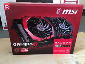
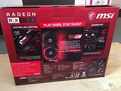
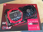
MSI Radeon RX 570 Gaming X Pictured

Someone got lucky with an early purchase of an MSI Radeon RX 570 Gaming X graphics card, ahead of its April 18th launch, and wasted no time in posting pictures of it, before selling it off on eBay for $329. Pictures reveal the card to look not much different from the RX 470 Gaming X, given that it features the same TwinFrozr VI cooling solution. This particular card features 4 GB of GDDR5 memory. While the box doesn't reveal clock speeds, it highlights "3rd gen FinFET 14" technology, proving that AMD is building the RX 570 and RX 580 chips on a newer, more advanced 14 nm FinFET node than the one it built Polaris 10 "Ellesmere" on.

AMD Readies Radeon RX 490 for December?

A spectacular rumor doing rounds has AMD sign 2016 off with a new high-end graphics card launch. The company could launch the Radeon RX 490 by the end of the year, according to an Guru3D report. This SKU could either be based on the larger Vega 10 silicon, or be a dual-GPU on a stick graphics card based on a pair of Polaris 10 "Ellesmere" chips. The former seems more likely as multi-GPU support among recent AAA game launches is dwindling. Earlier this year, AMD inadvertently leaked the SKU name Radeon RX 490 on its website.

If the Radeon RX 490 is based on the Vega 10, then it could feature 4,096 stream processors based on the "Vega" architecture, 256 TMUs, 64 ROPs, and a 4096-bit HBM2 memory interface, holding 8 GB or 16 GB of memory, with a memory bandwidth of 512 GB/s. If instead it is a dual-GPU card based on Polaris 10, then you could be looking at 2x 2,304 stream processors, and 16 GB of GDDR5 memory across two 256-bit wide memory interfaces.

PowerColor Intros the Radeon RX 470 Red Dragon V2 Graphics Card

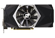
PowerColor unveiled the Radeon RX 470 Red Dragon V2 4 GB graphics card (model: AXRX470 4GBD5-3DHDV2/OC). A cost-effective variant of the original RX 470 Red Dragon, this card features a simpler single-fan cooling solution. The cooler features an aluminium fin-heatsink milled from a single chunk of metal; with a copper core, and two copper heat pipes that make direct contact with the GPU, quickly pushing heat to the edges of the heatsink. This heatsink also makes contact with the VRM MOSFETs. A single 100 mm fan ventilates the heatsink.

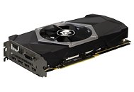
The PowerColor Radeon RX 470 Red Dragon V2 is factory-overclocked, with engine clocks up to 1206 MHz, and 6.60 GHz (GDDR5-effective) memory; which are the same as the original (dual-fan) RX 470 Red Dragon. The card features 4 GB of GDDR5 memory across the chip's 256-bit wide memory interface. Based on the Polaris 10 "Ellesmere" silicon, the Radeon RX 470 features 2,048 stream processors, 128 TMUs, and 32 ROPs. The card draws power from a single 6-pin PCIe power connector. PowerColor could price this card around the $170 mark.

AMD Reveals Three Entries on the WX Series Lineup: WX4100, WX5100 and WX7100

At its WX call, AMD focused on shifts in creativity from traditional design flows such as Solidworks, Adobe and Autodesk towards game engines as solutions for design visualization (Unreal Engine, Unity, CryEngine, or Autodesk's own Stingray platform), which signal changes in the creator ecosystem. Thanks to globalization, the Internet, and the available wealth of knowledge one can access through it, the line between amateurs and professionals is becoming more and more blurred. Now, those who would once be called amateurs are also using professional tools, and AMD plans to be at the forefront of technologies empowering creators to deliver their vision.

Radeon PRO serves to give creators more flexible and powerful solutions, leveraging open-source resources and centering the ecosystem back on creators and the tools they choose to use, with focused support on VR. As such, AMD is giving them the tools they need, by introducing three new products featuring the Polaris architecture, including 3 year standard + 7 year free extended warranty (including components such as the PCB itself, the PCI-Express slot, and the heatsinks), with AMD taking that extra 7 years as company commitment towards the quality of their products. Those three products are the WX4100, the WX5100, and the WX7100, and have planned, staggered availability throughout November.

Two Interesting AMD Prototypes Logged at Hyderabad Air Cargo

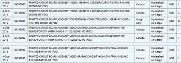
The air cargo hub at Hyderabad International Airport in India, is where interesting hardware prototypes make a connection between long-haul cargo planes coming from the far-east, to Europe, and North America. Zauba sniffed out transit records of two AMD prototypes earlier this month; beginning with "Dracarys." You probably remember that as the fictional command given by "Game of Thrones" characters to make dragons breathe fire.

This is further described as having a "Fiji" ASIC and "SSD," indicating that this could be one of AMD's Radeon Pro SSG, graphics cards which use onboard SSDs as additional frame-buffer. Next up, is an "Ellesmere XT MXM." This is a mobile graphics MXM board with a full-fledged Polaris 10 "Ellesmere" ASIC. It could have all 2,304 stream processors enabled, even if not having the same clocks as the desktop Radeon RX 480.

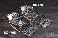
Sapphire Radeon RX 470D NITRO Pictured, Beats GTX 1050 Ti

It turns out that the new SKU based on the Polaris 10 "Ellesmere" silicon AMD is working on, to fill the gap between the Radeon RX 460 and RX 470, could be named the "Radeon RX 470D," after all. It is also being reported that AMD is planning to launch this SKU only in China, for now. It is further cut down from the RX 470, in featuring 1,792 stream processors, by enabling just 28 out of 36 GCN compute units physically present on the chip. The SKU further features 112 TMUs, 32 ROPs, and 4 GB of GDDR5 memory across a 256-bit wide memory interface.

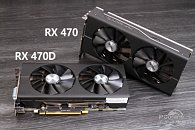
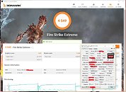
AMD is clocking the RX 470D slightly higher than the conventional RX 470. Its core ticks at speeds of up to 1266 MHz (Boost clock), and its memory at 7.00 GHz (GDDR5-effective), compared to the 1206 MHz (Boost clock) and 6.60 GHz (GDDR5-effective) speeds of the RX 470. The RX 470D will be built to a cost, and it shows, on the Sapphire RX 470D NITRO. The PCB is shorter, and the cooler leaner. Chinese tech publication PCOnline got its hands on a sample, and tested it to be faster than the GeForce GTX 1050 Ti, yet slower than the RX 470. The card is expected to be priced about 14 percent less than the RX 470. Find more benchmark figures in the PCOnline review linked below.
AMD Readying an Answer to GeForce GTX 1050 Ti

With the arrival of the GeForce GTX 1050 Ti and GTX 1050, the sub-$150 graphics card market is beginning to heat up. AMD is finding itself with a price-performance gorge between the Radeon RX 460 and the RX 470. Citing multiple sources, VideoCardz suspects that AMD is up to something - a new Polaris 10 "Ellesmere" based SKU positioned between the RX 460 and RX 470, referred to either as the "RX 465" or the "RX 470 SE."

The new SKU is further cut down from the Polaris 10 stack, in a bid to lower TDP below the 100W mark, to around 90W. The chip features 1,792 stream processors across 28 Graphics CoreNext compute units (CUs), out of the 36 CUs physically present on the chip. The RX 470 features 32 CUs, while the RX 480 maxes out all available CUs. AMD is leaving the memory bus untouched. It features 4 GB of GDDR5 memory across a 256-bit wide memory interface, ticking at 7.00 GHz (GDDR5-effective), churning up 224 GB/s of memory bandwidth - double that of the GTX 1050 series. There's also talk of yet another SKU, with 1,536 stream processors (24/36 CUs enabled), which AMD could position against the GTX 1050 (non-Ti).

AMD Polaris 10 "Ellesmere" Die Shot Confirms Max Shader Count

An AMD Polaris 10 "Ellesmere" based graphics card (RX 470 or RX 480) was taken apart down to its die, for science. Close up die-shots of the silicon reveal that 36 GCN compute units is all that the silicon has, and that the RX 480 indeed maxes out this stream processor count, with 2,304 stream processors at its disposal.

The die is fabbed by GlobalFoundries, on its swanky new 14 nm FinFET process. Redditors good at pattern-recognition could make out 36 "structures" spread across four quadrants, deducing them to be the GCN compute units. Each of these CUs feature 64 stream processors. Roadmaps reveal that the next high-end GPUs by AMD could be based on its newer "Vega" architecture.

AMD Radeon RX 470 and RX 460 Official Specifications Leaked

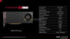
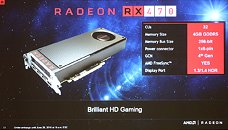
The official specifications of two the two upcoming mainstream graphics cards by AMD, the Radeon RX 470, and the Radeon RX 460, were leaked to the web as slides from the company's official press presentation ahead of their early-August product launches. The RX 470 is based on the same "Ellesmere" Polaris10 silicon as the RX 480. It features 2,048 stream processors across 32 GCN compute units; 128 TMUs, 32 ROPs, and 4 GB of memory across a 256-bit wide GDDR5 memory interface.

The RX 470 features clock speeds of 926 MHz core, 1206 MHz boost, and 6.6 Gbps memory, working out to 211 GB/s memory bandwidth. The RX 460, on the other hand, is based on the "Baffin" Polaris11 silicon, featuring 896 stream processors, 48 TMUs, 16 ROPs, and 4 GB of memory across a 128-bit wide GDDR5 memory interface. Its core is clocked at 1090 MHz, with 1200 MHz boost, and 7 Gbps memory, working out to 112 GB/s memory bandwidth. The RX 470 draws power from a single 6-pin PCIe power connector as its TDP is rated at 120W; the RX 460 relies entirely on the PCIe slot for its power, as its TDP is rated at <75W. The RX 470 will be available from 4th August, 2016; with the RX 460 following on 8th August.

AMD Radeon RX 470 and RX 460 Specifications Confirmed

AMD confirmed specifications of its second and third "Polaris" architecture graphics cards in a leaked presentation, the Radeon RX 470, and the Radeon RX 460. The RX 470 will be AMD's attempt at a graphics card that plays everything at 1080p resolution, under $150. The Radeon RX 460, on the other hand, is based on the new 14 nm Polaris11 "Baffin" silicon, and could be ideal for MOBA games with light GPU requirements.

The Radeon RX 470 is carved out from the Polaris10 "Ellesmere" silicon that the RX 480 is based on, it features 2,048 stream processors across 32 GCN compute units, 128 TMUs, 32 ROPs, and a 256-bit wide GDDR5 memory interface, holding 4 GB of memory. The card draws power from a single 6-pin PCIe power connector. The Radeon RX 460, on the other hand, features 896 stream processors across 14 compute units, 2 GB of GDDR5 memory across a 128-bit wide memory interface, and relies on the PCI-Express slot entirely for power. The reference RX 460 board looks quite similar to the Radeon R9 Nano, but features a simpler spiral heatsink under the fan. Despite rumors to the contrary, it looks like Vega is on-course for a 2017 launch after all.

Sapphire Reference Radeon RX 480 Taken Apart, Pictured Some More

A Sapphire branded AMD reference design Radeon RX 480 graphics card was taken apart, giving us an early close look at the card and its key components. The pictures reveal pretty much the same details as the first close-up shot of the reference RX 480 / RX 470 common PCB, and the cooling solution was taken apart further, revealing more details than the first time we saw what's underneath.

To begin with, the reference RX 480 PCB features a 6-phase VRM that draws power from a single 6-pin PCIe power connector. Display outputs include one HDMI 2.0 and three DisplayPort 1.4 connectors. One of the pictures features a close-up of the 14 nm "Ellesmere" silicon. The cooling solution is confirmed to feature a chunky monolithic aluminium heatsink with a copper core, cooling the GPU, with a metal base-plate conveying heat from the VRM and memory to it; ventilated by a lateral blower. The Radeon RX 480 is expected to launch on the 29th of June, 2016, priced at $199 for the 4 GB variant, and $229 for the 8 GB variant.
More pictures follow.

XFX Radeon RX 480 Pictured on its Production Line

Here's a sight for sore eyes, a stream of Radeon RX 480 graphics cards by XFX are making their way down the production line to packaging. The picture reveals that XFX could top up the reference-design RX 480 board with a back-plate, to make it even more marketable. To give you an idea of just how cool the 14 nm "Ellesmere" chip runs, with the cooler shroud taken apart, you'll find that the GPU is cooled by just a chunky, monolithic aluminium heatsink with a copper core, and not an elaborate aluminium fin-stack/channel setup with heat-pipes crisscrossing it. A base-plate cools the memory and VRM. In related news, ChipHell scored a GPU-Z screenshot of the XFX Radeon RX 480, confirming its stream processor count of 2,304 and GPU clocks of 1328 MHz, with the memory ticking at 8 GHz (GDDR5-effective).

AMD "Ellesmere" ASIC Pictured Up Close in RX 480 PCB Picture Leak

AMD's all-important Polaris10 "Ellesmere" ASIC is pictured up close in a 3-quarter PCB shot of the upcoming Radeon RX 480 / RX 470. The picture reveals the ASIC with a die that's significantly smaller than that of the 28 nm "Tonga" silicon. The "Ellesmere" die is built on the 14 nm FinFET+ process. The die is seated on a substrate with a 256-bit wide GDDR5 memory interface. This appears to be a common reference PCB between the RX 480 and the RX 470.

The RX 480 ships with a classy looking lateral-flow cooler that's longer than the PCB itself; while the RX 470 uses a more common fin-stack top-flow cooling solution. Of course both cards are expected to ship with custom-design boards and cooling solutions. The reference PCB draws power from a single 6-pin PCIe power connector, and uses a 6-phase VRM to condition it for the GPU and memory. Display outputs include three DisplayPort 1.4 and one HDMI 2.0a connectors. There are also unused traces on the PCB for a DVI connector, so it's likely that some custom-design cards could feature it.

AMD Confirms "Ellesmere" and "Baffin" GPU Specs

In its post-E3 press-deck, AMD confirmed the specifications of its Polaris10 "Ellesmere" and Polaris11 "Baffin" GPUs. The two chips will drive at least three desktop discrete SKUs between them, the Radeon RX 480, the RX 470, and the RX 460. Of these, the RX 480 and RX 470 appear to be based on the "Ellesmere" silicon. This chip features 2,304 stream processors spread across 36 compute units (CUs), and a 256-bit wide GDDR5 memory interface. The "Baffin" silicon, on the other hand, features 1,024 stream processors spread across 16 CUs, and a 128-bit GDDR5 memory interface, likely ticking at 128 GB/s.

AMD Radeon RX 480 "Polaris" Launched at $199

AMD made a bold move in launching its first "Polaris" architecture based performance-segment GPU, the Radeon RX 480 at a starting price of US $199. The company claims that it will perform on-par with $500 graphics cards from the previous generation, directly hinting at performance being on par with the Radeon R9 Fury and R9 Nano. Although it's not in the league of the GTX 1070 or the GTX 1080, this level of performance at $199 could certainly disrupt things for NVIDIA, as it presents an attractive option for people still gaming on 1440p and 1080p resolutions (the overwhelming majority). The R9 Fury can handle any game at 1440p.

The Radeon RX 480 is based on the 14 nm "Ellesmere" silicon, fabbed by GlobalFoundries. It's publicly known that GloFlo has a 14 nm fab in Malta (upstate New York), USA. The RX 480 is based on AMD's 4th generation Graphics CoreNext architecture, codenamed "Polaris." It features 2,304 stream processors, spread across 36 compute units (CUs). Its single-precision floating point performance is rated by AMD to be "greater than 5 TFLOP/s." The chip features a 256-bit wide GDDR5 memory interface, with memory clocked at 8 Gbps, yielding memory bandwidth of 256 GB/s. There will be two variants of this card, 4 GB and 8 GB. It's the 4 GB variant that starts at $199, the 8 GB variant is expected to be priced at $229. AMD confirmed that the GPU will support DisplayPort 1.4 although it's certified up to DisplayPort 1.3. The typical board power is rated at 150W. The card could be available from 29th June.

More Polaris10 and Polaris11 Specifications Revealed

Industry sources revealed to TechPowerUp some pretty interesting specifications of AMD's two upcoming GPUs based on the 4th generation Graphics CoreNext "Polaris" architecture. The company is preparing a performance-segment GPU and a mainstream one. It turns out, that the performance-segment chip, which the press has been referring to as "Ellesmere," could feature 32 compute units (CUs), and not the previously thought 40.

Assuming that each CU continues to consist of 64 stream processors (SP), you're looking at an SP count of 2,048. What's more, this chip is said to offer a single-precision floating point performance of 5.5 TFLOP/s, as claimed by AMD. To put this into perspective, the company had claimed 5.2 TFLOP/s for the "Hawaii"/"Grenada" based FirePro W9100, which launched earlier this February, and that SKU featured all 2,816 SP present on the chip. So this chip is definitely faster than most "Hawaii" based SKUs.

AMD to Launch First "Polaris" Graphics Cards by Late May

The first AMD Radeon graphics cards based on the company's "Polaris" architecture are slated for a late-May launch, according to Thai tech-site Zolkorn. The company is reportedly planning an elaborate launch event in Macau, China, days ahead of the 2016 Computex trade-show in Taipei. AMD has reportedly already sent invites to media outlets, although to a very limited number (in comparison to, say, NVIDIA's GTX 1080 event in Austin, US). The event could see a paper-launch of the first Radeon R9 400 series graphics cards based on the 14 nm "Ellesmere" and "Baffin" chips, with AIB-branded cards being exhibited at Computex, and market-availability following shortly after.

AMD Radeon R9 480 (non-X) Performs Close to R9 390X

In all the 16 nm NVIDIA "Pascal" GPU fervor, it would be foolish to ignore AMD's first "Polaris" GPUs, built on the more advanced 14 nm process. Hot on the heels of reports that a fully-equipped "Ellesmere" GPU based Radeon R9 490 performs close to NVIDIA's GeForce GTX 980 Ti (and AMD's own R9 Fury X), with nearly half its power-draw, new numbers from an early GFXBench run suggests that its cut-down R9 480 (non-X) sibling performs close to the Radeon R9 390X. The R9 480 succeeds the currently-$200 R9 380, and its prospect of offering performance rivaling the $400 R9 390X at half its power-draw appears to meet AMD's "generational leap" claims for the "Polaris" architecture. Similarly, the R9 490, based on a better-endowed "Ellesmere" chip, offering performance rivaling current $600 GPUs at a $350-ish price-point (succeeding the R9 390), appears to meet expectations of a generation leap.

AMD Teases Polaris 10 and Polaris 11 ASIC Images

AMD posted a new webpage for its upcoming "Polaris" GPU architecture, outlining its various innovations - 4th gen. Graphics CoreNext, 4K H.265 60 Hz game-streaming, next-generation display engine with support for DisplayPort 1.3 and HDMI 2.0, XConnect Technology, and the foundation of GPUOpen. In this page, the company inadvertently leaked pictures of its upcoming Polaris 10 "Ellesmere" and Polaris 11 "Baffin" ASICs.

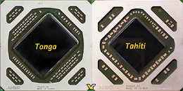
The mast image of the page has a faded 3-quarter shot of a "small" GPU with a die that's almost 30% of the package area. This hints at Polaris 11 "Baffin." This chip is rumored to feature a 128-bit GDDR5/GDDR5X memory interface, and so its pin-count, and conversely, package-size is less. Then in its "4th gen GCN" heading image, AMD showed a picture of a bigger GPU. At first glance, you could assume that it's either "Tonga XT" or "Tahiti" looking at its support brace, but VideoCardz observed that the on-package electrical components in this image are arranged nothing like on the "Tonga" or "Tahiti." This could very well be Polaris 10 "Ellesmere."

AMD Polaris 10 "Ellesmere" as Fast as GTX 980 Ti: Rumor

At a presser in Taiwan for its Radeon Pro Duo launch, AMD talked extensively about its upcoming "Polaris" and "Vega" family of GPUs. The company appears to be betting heavily on two SKUs it plans to launch this June, Polaris 10 and Polaris 11. Polaris 10 is an internal designation to Radeon R9 490(X), based on the 14 nm "Ellesmere" silicon. It may be the biggest chip AMD builds on the "Polaris" architecture, but it won't exactly be a "big chip," in that it doesn't succeed "Fiji." That honor is reserved for "Vega," which debuts in early-2017.

The "Ellesmere" silicon is more of AMD's competitor to NVIDIA's GP104. It is rumored that the R9 490(X), based on this silicon, will offer consumers performance rivaling the GeForce GTX 980 Ti (ergo faster than the Radeon R9 Fury X), at a USD $300-ish price point. "Ellesmere" will be a lean-machine, physically featuring up to 2,560 4th generation GCN stream processors (2,304 enabled on Polaris 10), a possible 256-bit GDDR5X memory interface, and a deep sub-200W typical board power rating.

AMD's GPU Roadmap for 2016-18 Detailed

AMD finalized the GPU architecture roadmap running between 2016 and 2018. The company first detailed this at its Capsaicin Event in mid-March 2016. It sees the company's upcoming "Polaris" architecture, while making major architectural leaps over the current-generation, such as a 2.5-times performance/Watt uplift and driving the company's first 14 nanometer GPUs; being limited in its high-end graphics space presence. Polaris is rumored to drive graphics for Sony's upcoming 4K Ultra HD PlayStation, and as discrete GPUs, it will feature in only two chips - Polaris 10 "Ellesmere" and Polaris 11 "Baffin."

"Polaris" introduces several new features, such as HVEC (h.265) decode and encode hardware-acceleration, new display output standards such as DisplayPort 1.3 and HDMI 2.0; however, since neither Polaris 10 nor Polaris 11 are really "big" enthusiast chips that succeed the current "Fiji" silicon, will likely make do with current GDDR5/GDDR5X memory standards. That's not to say that Polaris 10 won't disrupt current performance-thru-enthusiast lineups, or even have the chops to take on NVIDIA's GP104. First-generation HBM limits the total memory amount to 4 GB over a 4096-bit path. Enthusiasts will have to wait until early-2017 for the introduction of the big-chip that succeeds "Fiji," which will not only leverage HBM2 to serve up vast amounts of super-fast memory; but also feature a slight architectural uplift. 2018 will see the introduction of its successor, codenamed "Navi," which features an even faster memory interface.

PlayStation 4K to Feature a 2,304-SP AMD "Polaris" GPU

Sony's upcoming 4K Ultra HD game console, which its fans are referring to as the "PlayStation 4K," while being internally referred to by Sony as "NEO," could feature a very powerful GPU. AMD could custom-design the SoC that drives the console, to feature an 8-core 64-bit x86 CPU based on the "Jaguar" micro-architecture, running at 2.10 GHz; and a GPU component featuring 36 compute units based on "next-generation Graphics CoreNext" architecture.

36 next-gen GCN compute units sounds an awful lot like the specs of the Polaris10 "Ellesmere" chip in its Radeon R9 480 configuration, working out to a stream processor count of 2,304 - double that of the 1,152 on the current-gen PlayStation 4. The SoC is also rumored to feature a 256-bit GDDR5 memory interface holding 8 GB of memory. This memory will be used as both system and video memory, just like on the current-gen PlayStation 4. The memory bandwidth will be increased to 218 GB/s from the current 176 GB/s. Besides 4K Ultra HD gaming, this chip could also prepare Sony for VR headsets, leveraging AMD's LiquidVR tech.

AMD to Launch Radeon R7 470 and R9 480 at Computex

Computex 2016 could see some major consumer graphics action, with AMD reportedly planning to launch two mid-thru-performance segment products on the sidelines of the event - the Radeon R7 470, based on the 14 nm "Baffin" (Polaris 11) silicon, and the Radeon R9 480, based on the 14 nm "Ellesmere" (Polaris 10) silicon. The R7 470 could succeed the R7 370 series in not just performance, but also offer a leap in energy efficiency, with a TDP of less than 50W. The R9 480, on the other hand, could feature a TDP of just 110-135W (R9 380 is rated at 190W).

The R9 480, based on the "Ellesmere" (Polaris 10) is shaping up to be a particularly interesting silicon. It's rumored to feature 2,304 stream processors based on the 4th generation Graphics CoreNext architecture, with 2,560 stream processors being physically present on the chip; and a 256-bit wide GDDR5 (GDDR5X-ready) memory controller. 8 GB could be the standard memory amount. AMD could keep the clock speeds relatively low, with 800-1050 MHz GPU clocks. Imagine R9 390-like performance at half its power-draw.

Upcoming AMD "Polaris" and "Vega" GPU Compute Unit Counts Surface

AMD's upcoming GPUs based on the "Polaris" and "Vega" architectures appear to be taking advantage of performance/Watt gains to keep stream processor counts low, and chips small, according to a VideoCardz analysis of curious-looking CompuBench entries. Assuming that a Graphics CoreNext (GCN) compute unit (CU) of the "Polaris" architecture, like the three versions of GCN before it, consists of 64 stream processors, AMD's Polaris 11 silicon, codenamed "Baffin," could feature over 1,024 stream processors, across 16 CUs; Polaris 10, codenamed "Ellesmere," could feature over 2,304 stream processors spread across over 36 CUs; and Vega 10 featuring 4,096 stream processors, spread across 64 CUs.

The "Baffin" silicon succeeds current generation "Curacao" silicon, driving mid-range graphics cards. It is expected to feature a 128-bit wide GDDR5 memory interface, holding 4 GB of memory. The "Ellesmere" silicon succeeds current-generation "Tonga" silicon, driving performance-segment SKUs. It could feature up to 8 GB of GDDR5(X) memory. These two chips could see the light of the day by mid-2016. The third chip out of AMD's stable, Vega 10, could succeed "Fiji," overcoming its biggest marketing shortcoming - 4 GB memory. Taking advantage of HBM2 interface, it could feature 16 GB of memory. It could launch some time in early-2017. AMD is claiming a massive 2.5X performance-per-Watt increase for "Polaris" over the current GCN 1.2 architecture, which drives the "Tonga" and "Fiji" chips, and so these stream processor counts could look deceptively insufficient.
Return to Keyword Browsing
Jan 21st, 2025 05:50 EST change timezone

New Forum Posts

Popular Reviews

Controversial News Posts