Monday, June 5th 2017

AMD "Vega" Die-shot Revealed
AMD released the die-shot of its "Vega 10" ASIC. The multi-chip module (MCM) of the GPU die and two HBM2 memory stacks, sitting on a silicon interposer, is slightly smaller than the "Fiji" ASIC, as it features just two memory stacks. AMD didn't label the components of the GPU die, but we can make out 8 shader engines, holding 8 GCN compute units (CUs), each. This is unlike "Fiji," where the GPU holds four engines with 16 CUs, each. This would mean that each group of 8 CUs has its own dedicated geometry processor and rasterizer.
Since each CU holds 64 FP32 stream processors, we arrive at the total stream processor count of 4,096. Unlike "Hawaii," these stream-processors are FP16-capable, so simple compute tasks are handled at double the throughput. We also make out 32 render back-ends, double that of "Fiji" and "Hawaii," which could indicate 128 ROPs. The "Vega 10" ASIC features a 2048-bit HBM2 memory interface.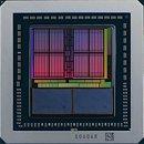
Update: AMD stated that the die-shot appeared in one of its marketing slides, but may not be real.
Since each CU holds 64 FP32 stream processors, we arrive at the total stream processor count of 4,096. Unlike "Hawaii," these stream-processors are FP16-capable, so simple compute tasks are handled at double the throughput. We also make out 32 render back-ends, double that of "Fiji" and "Hawaii," which could indicate 128 ROPs. The "Vega 10" ASIC features a 2048-bit HBM2 memory interface.

16 Comments on AMD "Vega" Die-shot Revealed
Yeah I mean this will easily compete with the 1080 Ti. Will likely match the Titan XP if they can hit 1.7GHz and 512 GB/s in the gaming cards.
Anyway, this gpu was rumoured even before Fury X was around.www.hardware.fr/focus/109/comprendre-memoire-hbm-introduite-par-amd.html
This part was covered (see pic) but one could easily see the shape of the chip, and it's quite similar to this, IMO.
If so, not beating it won't be such a big deal.