Monday, August 20th 2018

NVIDIA GeForce RTX 2080 ASIC is "TU104," Smiles for the Camera
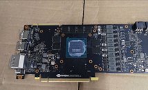
Here are some of the first pictures of the "TU104," the chip at at heart of NVIDIA GeForce RTX 2080, in its top-spec TU104-400A-A1 variant. While the package itself isn't bigger than that of its predecessors, the GP104 and GM204, the die of the TU104 is huge! If it's built on existing silicon fabrication processes such as 14 nm or 12 nm, the TU104 could end up with transistor-counts higher than those of even the GP102.
You'll recall that we posted bare-PCB pictures of this board recently. In its production (or close-to-production) variant, the board draws power from a combination of 6-pin and 8-pin PCIe connectors, conditioning it with an 8+2 phase VRM. The GPU is surrounded by eight GDDR6 memory chips. Display connectivity includes three DisplayPorts, an HDMI, and a USB type-C (VirtuaLink).
You'll recall that we posted bare-PCB pictures of this board recently. In its production (or close-to-production) variant, the board draws power from a combination of 6-pin and 8-pin PCIe connectors, conditioning it with an 8+2 phase VRM. The GPU is surrounded by eight GDDR6 memory chips. Display connectivity includes three DisplayPorts, an HDMI, and a USB type-C (VirtuaLink).


10 Comments on NVIDIA GeForce RTX 2080 ASIC is "TU104," Smiles for the Camera
And that definitely looks like a blower style cooler, guess that reference design render probably is fake.
This GPU is meant for 7nm, 500 mm2 gets shrinked to 300mm2 like normal. And the clocks at 7nm are 1.40x higher. So why release this GPU now.