Wednesday, October 31st 2018

AMD Could Solve Memory Bottlenecks of its MCM CPUs by Disintegrating the Northbridge
AMD sprung back to competitiveness in the datacenter market with its EPYC enterprise processors, which are multi-chip modules of up to four 8-core dies. Each die has its own integrated northbridge, which controls 2-channel DDR4 memory, and a 32-lane PCI-Express gen 3.0 root complex. In applications that can not only utilize more cores, but also that are memory bandwidth intensive, this approach to non-localized memory presents design bottlenecks. The Ryzen Threadripper WX family highlights many of these bottlenecks, where video encoding benchmarks that are memory-intensive see performance drops as dies without direct access to I/O are starved of memory bandwidth. AMD's solution to this problem is by designing CPU dies with a disabled northbridge (the part of the die with memory controllers and PCIe root complex). This solution could be implemented in its upcoming 2nd generation EPYC processors, codenamed "Rome."
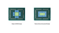
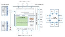
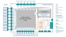
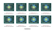
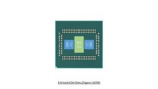
With its "Zen 2" generation, AMD could develop CPU dies in which the integrated northrbidge can be completely disabled (just like the "compute dies" on Threadripper WX processors, which don't have direct memory/PCIe access relying entirely on InfinityFabric). These dies talk to an external die called "System Controller" over a broader InfinityFabric interface. AMD's next-generation MCMs could see a centralized System Controller die that's surrounded by CPU dies, which could all be sitting on a silicon interposer, the same kind found on "Vega 10" and "Fiji" GPUs. An interposer is a silicon die that facilitates high-density microscopic wiring between dies in an MCM. These explosive speculative details and more were put out by Singapore-based @chiakokhua, aka The Retired Engineer, a retired VLSI engineer, who drew block diagrams himself.The System Controller die serves as town-square for the entire processor, and packs a monolithic 8-channel DDR4 memory controller that can address up to 2 TB of ECC memory. Unlike current-generation EPYC processors, this memory interface is truly monolithic, much like Intel's implementation. The System Controller also features a PCI-Express gen 4.0 x96 root-complex, which can drive up to six graphics cards with x16 bandwidth, or up to twelve at x8. The die also integrates the southbridge, known as Server Controller Hub, which puts out common I/O interfaces such as SATA, USB, and other legacy low-bandwidth I/O, in addition to some more PCIe lanes. There could still be external "chipset" on the platform that puts out more connectivity.The Retired Engineer goes on to speculate that AMD could even design its socket AM4 products as MCMs of two CPU dies sharing a System Controller die; but cautioned to take it with "a bowl of salt." This is unlikely given that the client-segment has wafer-thin margins compared to enterprise, and AMD would want to build single-die products - ones in which the integrated northbridge isn't disabled. Still, that doesn't completely discount the possibility of a 2-die MCM for "high-margin" SKUs that AMD can sell around $500. In such cases, the System Controller die could be leaner, with fewer InfinityFabric links, a 2-channel memory I/O, and a 32-lane PCIe gen 4.0 root.AMD will debut the "Rome" MCM within 2018.
Source:
The Retired Engineer
With its "Zen 2" generation, AMD could develop CPU dies in which the integrated northrbidge can be completely disabled (just like the "compute dies" on Threadripper WX processors, which don't have direct memory/PCIe access relying entirely on InfinityFabric). These dies talk to an external die called "System Controller" over a broader InfinityFabric interface. AMD's next-generation MCMs could see a centralized System Controller die that's surrounded by CPU dies, which could all be sitting on a silicon interposer, the same kind found on "Vega 10" and "Fiji" GPUs. An interposer is a silicon die that facilitates high-density microscopic wiring between dies in an MCM. These explosive speculative details and more were put out by Singapore-based @chiakokhua, aka The Retired Engineer, a retired VLSI engineer, who drew block diagrams himself.The System Controller die serves as town-square for the entire processor, and packs a monolithic 8-channel DDR4 memory controller that can address up to 2 TB of ECC memory. Unlike current-generation EPYC processors, this memory interface is truly monolithic, much like Intel's implementation. The System Controller also features a PCI-Express gen 4.0 x96 root-complex, which can drive up to six graphics cards with x16 bandwidth, or up to twelve at x8. The die also integrates the southbridge, known as Server Controller Hub, which puts out common I/O interfaces such as SATA, USB, and other legacy low-bandwidth I/O, in addition to some more PCIe lanes. There could still be external "chipset" on the platform that puts out more connectivity.The Retired Engineer goes on to speculate that AMD could even design its socket AM4 products as MCMs of two CPU dies sharing a System Controller die; but cautioned to take it with "a bowl of salt." This is unlikely given that the client-segment has wafer-thin margins compared to enterprise, and AMD would want to build single-die products - ones in which the integrated northbridge isn't disabled. Still, that doesn't completely discount the possibility of a 2-die MCM for "high-margin" SKUs that AMD can sell around $500. In such cases, the System Controller die could be leaner, with fewer InfinityFabric links, a 2-channel memory I/O, and a 32-lane PCIe gen 4.0 root.AMD will debut the "Rome" MCM within 2018.

60 Comments on AMD Could Solve Memory Bottlenecks of its MCM CPUs by Disintegrating the Northbridge
Im just saying this because im not sure if more then one memory controller is beneficial at all when you have a multi cpu setup...
I know... its a bit out of the box but yeah
For reference, checkout the last paragraph here for on overview of the current implementation: en.wikichip.org/wiki/amd/infinity_fabric
Well... thought it may be a better idea to just combine the memory controllers into one big die. One you can upgrade, the same way as you can with cpu`s.
Btw, welcome to TPU ;)
Im not saying that this is the solution. its just that with thinking out of the box one might find new ways to improve their product.
and thanks bug
AMD brought most of this on themselves, technical issues with ZEN, bulldozer, and other designs and latency to cache and memory has never truly been solved for years and "add more cores" has always been the solution. They need to build a memory controller for a 8 core that can be expanded to these insane core and thread counts, where a little latency added to a server workload with custom aware of penalties software handling the threads can mask it.
Most applications are very sensitive to memory latency, so redesigning this approach in future Zen iterations seems like a very good idea. Keeping cache and memory controllers as efficient and low latency as possible is one of the keys to increasing IPC.
Even in may there were already rumours of a similar idea being passed around at intel, however as we all know intel is very far behind on the whole MCM architecture and as such it will be at least a year before any of their offerings are even doing the rounds being sampled before their retail release.
This is the way forward for the high end CPU market and anyone who says it isn't is just impossibly deluded...
I hope to see AMD continue their competitive streak in the high end, they have set high targets but I am pretty sure they will be achieved. I also hope they put a bit more time into refining the 8 core and lower chips to be more competitive on the gaming side.
forums.anandtech.com/threads/64-core-epyc-rome-%EF%BC%88zen2%EF%BC%89architecture-overview%EF%BC%9F.2554453/page-14#post-39633456