Wednesday, October 31st 2018

AMD Could Solve Memory Bottlenecks of its MCM CPUs by Disintegrating the Northbridge
AMD sprung back to competitiveness in the datacenter market with its EPYC enterprise processors, which are multi-chip modules of up to four 8-core dies. Each die has its own integrated northbridge, which controls 2-channel DDR4 memory, and a 32-lane PCI-Express gen 3.0 root complex. In applications that can not only utilize more cores, but also that are memory bandwidth intensive, this approach to non-localized memory presents design bottlenecks. The Ryzen Threadripper WX family highlights many of these bottlenecks, where video encoding benchmarks that are memory-intensive see performance drops as dies without direct access to I/O are starved of memory bandwidth. AMD's solution to this problem is by designing CPU dies with a disabled northbridge (the part of the die with memory controllers and PCIe root complex). This solution could be implemented in its upcoming 2nd generation EPYC processors, codenamed "Rome."
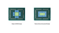
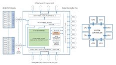
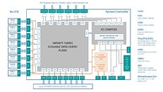
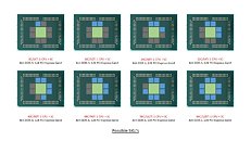
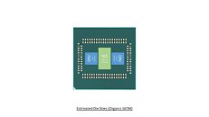
With its "Zen 2" generation, AMD could develop CPU dies in which the integrated northrbidge can be completely disabled (just like the "compute dies" on Threadripper WX processors, which don't have direct memory/PCIe access relying entirely on InfinityFabric). These dies talk to an external die called "System Controller" over a broader InfinityFabric interface. AMD's next-generation MCMs could see a centralized System Controller die that's surrounded by CPU dies, which could all be sitting on a silicon interposer, the same kind found on "Vega 10" and "Fiji" GPUs. An interposer is a silicon die that facilitates high-density microscopic wiring between dies in an MCM. These explosive speculative details and more were put out by Singapore-based @chiakokhua, aka The Retired Engineer, a retired VLSI engineer, who drew block diagrams himself.The System Controller die serves as town-square for the entire processor, and packs a monolithic 8-channel DDR4 memory controller that can address up to 2 TB of ECC memory. Unlike current-generation EPYC processors, this memory interface is truly monolithic, much like Intel's implementation. The System Controller also features a PCI-Express gen 4.0 x96 root-complex, which can drive up to six graphics cards with x16 bandwidth, or up to twelve at x8. The die also integrates the southbridge, known as Server Controller Hub, which puts out common I/O interfaces such as SATA, USB, and other legacy low-bandwidth I/O, in addition to some more PCIe lanes. There could still be external "chipset" on the platform that puts out more connectivity.The Retired Engineer goes on to speculate that AMD could even design its socket AM4 products as MCMs of two CPU dies sharing a System Controller die; but cautioned to take it with "a bowl of salt." This is unlikely given that the client-segment has wafer-thin margins compared to enterprise, and AMD would want to build single-die products - ones in which the integrated northbridge isn't disabled. Still, that doesn't completely discount the possibility of a 2-die MCM for "high-margin" SKUs that AMD can sell around $500. In such cases, the System Controller die could be leaner, with fewer InfinityFabric links, a 2-channel memory I/O, and a 32-lane PCIe gen 4.0 root.AMD will debut the "Rome" MCM within 2018.
Source:
The Retired Engineer
With its "Zen 2" generation, AMD could develop CPU dies in which the integrated northrbidge can be completely disabled (just like the "compute dies" on Threadripper WX processors, which don't have direct memory/PCIe access relying entirely on InfinityFabric). These dies talk to an external die called "System Controller" over a broader InfinityFabric interface. AMD's next-generation MCMs could see a centralized System Controller die that's surrounded by CPU dies, which could all be sitting on a silicon interposer, the same kind found on "Vega 10" and "Fiji" GPUs. An interposer is a silicon die that facilitates high-density microscopic wiring between dies in an MCM. These explosive speculative details and more were put out by Singapore-based @chiakokhua, aka The Retired Engineer, a retired VLSI engineer, who drew block diagrams himself.The System Controller die serves as town-square for the entire processor, and packs a monolithic 8-channel DDR4 memory controller that can address up to 2 TB of ECC memory. Unlike current-generation EPYC processors, this memory interface is truly monolithic, much like Intel's implementation. The System Controller also features a PCI-Express gen 4.0 x96 root-complex, which can drive up to six graphics cards with x16 bandwidth, or up to twelve at x8. The die also integrates the southbridge, known as Server Controller Hub, which puts out common I/O interfaces such as SATA, USB, and other legacy low-bandwidth I/O, in addition to some more PCIe lanes. There could still be external "chipset" on the platform that puts out more connectivity.The Retired Engineer goes on to speculate that AMD could even design its socket AM4 products as MCMs of two CPU dies sharing a System Controller die; but cautioned to take it with "a bowl of salt." This is unlikely given that the client-segment has wafer-thin margins compared to enterprise, and AMD would want to build single-die products - ones in which the integrated northbridge isn't disabled. Still, that doesn't completely discount the possibility of a 2-die MCM for "high-margin" SKUs that AMD can sell around $500. In such cases, the System Controller die could be leaner, with fewer InfinityFabric links, a 2-channel memory I/O, and a 32-lane PCIe gen 4.0 root.AMD will debut the "Rome" MCM within 2018.

60 Comments on AMD Could Solve Memory Bottlenecks of its MCM CPUs by Disintegrating the Northbridge
Thus one of the reasons this is genius
Together with the fact that on desktop and laptop the second (of two) chiplets will be a GPU...for entry-level, mainstream and mobile they'll keep 8C/16T, make it one chiplet (no CCX), interface to the NB and combine those 2 with a GPUactually, see above, it creates all the solutions...chiplet will be 8 cores with lower internal latency
plus:
-latency to RAM will be even for all MCM solutions
-it's easy to combine with a GPU for mainstream and mobileit will be a single design for all Zen, consisting of CPU^8 or CPU+GPU, it's kinda brilliant really
these days virtually no app is optimised for more than 8 cores thus the chiplet unit will have 8 cores all with low-latency communications via a 32MB L3you're right...it will be a single memory controller on the Northbridge that feeds all the CPU chiplets -and that's the beauty of it, the same latency to all chiplets plus a massive L4 cache...i'd wager the CCX is going to go all together and allow each chiplet to have 8 low-latency cores
after all the Northbridge will do most of the memory workthey will have a ring-bus but only for each 8-core chiplet...makes perfect sense, solve the latency issue for what is the standard number of cores whilst keeping it standard
then scale it OR +GPU it depending on platform
completely solves the Threadripper 32 core problems...every chiplet from Ryzen to EPYC will be the same
8-cores, ringbus, no CCX
massive L3 cache to offset memory latency likely together with a even more massive L4 cache on the memory controller
as to Threadripper, Dynamic Local Mode goes out the window as the OS just sees 4 equally-balanced CPU NUMA domains
the end result will be similar to the IBM approach except with another 2 layers of cache hierarchy to hide latency...L3 for the chiplets plus an L4 for the Northbridge
Second, interchiplet communications latency is lower in a true 8 core but memory latency will be higher if memory controller is in another die compared to on-die. One step forward, one step back.
Third, that massive L4 cache will be expensive to manufacture, especially harming the price of CPUs with just 1 chiplet.
Fourth, the main problem with 24/32 TR is that 2 of the 4 dies don't have direct access to the memory controller, now imagine none of them.
Fifth, if MCM is a solution for EPYC, it is not for Ryzen where costs should remain low (no L4) and low threaded performance high, so it is better to have different designs.
Sixth, the OS will see X number of equally-slower domains in Zen 2 compared to TR2.
-latency to eDRAM will be very low and give you your x1 for instructions; data can be prefetched, bandwidth not latency is the issue there
-in fact a large eDRAM has been done before and it's not that expensive, it's IrisPro or the GameCube (1T SRAM); combine yields@14nm plus salvage for eg 64MB vs 256MB and what does it really cost?
-adding all that together why still have such a large L4 on mainstream Ryzen? as above, it's to pair up Zen Chiplet with a Vega GPU -but with proper coherency because it's IF not Intel Graphics
-need to keep it really low cost at the low end? then ok, tweak and rebrand the 2700x into the 3600
will be exciting to see where this goes..looking forward to the event on the 6th!
Some tidbits:
More info and pics on the post @ Anandtech forums linked above.
There's also this from another post in the same topic:
AMD could potentially get around this as well.
There is some speculation based on the huge IO-Die that there might be a Large L4 cache.
If you have an L4 large enough to maintain a copy of all the Data in the 8x L3 caches.
Instead of getting the Data from another die's L3, just fetch it from the L4.