Wednesday, January 23rd 2019

Bulldozer Core-Count Debate Comes Back to Haunt AMD
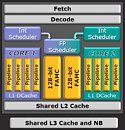
AMD in 2012 launched the FX-8150, the "world's first 8-core desktop processor," or so it says on the literal tin. AMD achieved its core-count of 8 with an unconventional CPU core design. Its 8 cores are arranged in four sets of two cores each, called "modules." Each core has its own independent integer unit and L1 data cache, while the two cores share a majority of their components - the core's front-end, a branch-predictor, a 64 KB L1 code cache, a 2 MB L2 cache, but most importantly, an FPU. There was much debate across tech forums on what constitutes a CPU core.
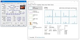
Multiprocessor-aware operating systems had to be tweaked on how to properly address a "Bulldozer" processor. Their schedulers would initially treat "Bulldozer" cores as fully independent (as conventional logic would dictate), until AMD noticed multi-threaded application performance bottlenecks. Eventually, Windows and various *nix kernels received updates to their schedulers to treat each module as a core, and each core as an SMT unit (a logical processor). The FX-8350 is a 4-core/8-thread processor in the eyes of Windows 10, for example. These updates improved the processors' performance but not before consumers started noticing that their operating systems weren't reporting the correct core-count. In 2015, a class-action lawsuit was filed against AMD for false marketing of FX-series processors. The wheels of that lawsuit are finally moving, after a 12-member Jury is set up to examine what constitutes a CPU core, and whether an AMD FX-8000 or FX-9000 series processor can qualify as an 8-core chip.US District Judge Haywood Gilliam of the District Court for the Northern District of California rejected AMD's claim that "a significant majority of" consumers understood what constitutes a CPU core, and that they had a fair idea of what they were buying when they bought AMD FX processors. AMD has two main options before it. The company can reach an agreement with the plaintiffs that could cost the company millions of Dollars in compensation; or fight it out in the Jury trial, by trying to prove to 12 members of the public (not necessarily from an IT background) what constitutes a CPU core and why "Bulldozer" qualifies as an 8-core silicon.
The plaintiffs and defendants each have a key technical argument. The plaintiffs could point out operating systems treating 8-core "Bulldozer" parts as 4-core/8-thread (i.e. each module as a core and each "core" as a logical processor); while the AMD could run multi-threaded floating-point benchmark tests to prove that a module cannot be simplified to the definition of a core. AMD's 2017 release of the "Zen" architecture sees a return to the conventional definition of a core, with each "Zen" core being as independent as an Intel "Skylake" core. We will keep an eye on this case.
Source:
The Register
Multiprocessor-aware operating systems had to be tweaked on how to properly address a "Bulldozer" processor. Their schedulers would initially treat "Bulldozer" cores as fully independent (as conventional logic would dictate), until AMD noticed multi-threaded application performance bottlenecks. Eventually, Windows and various *nix kernels received updates to their schedulers to treat each module as a core, and each core as an SMT unit (a logical processor). The FX-8350 is a 4-core/8-thread processor in the eyes of Windows 10, for example. These updates improved the processors' performance but not before consumers started noticing that their operating systems weren't reporting the correct core-count. In 2015, a class-action lawsuit was filed against AMD for false marketing of FX-series processors. The wheels of that lawsuit are finally moving, after a 12-member Jury is set up to examine what constitutes a CPU core, and whether an AMD FX-8000 or FX-9000 series processor can qualify as an 8-core chip.US District Judge Haywood Gilliam of the District Court for the Northern District of California rejected AMD's claim that "a significant majority of" consumers understood what constitutes a CPU core, and that they had a fair idea of what they were buying when they bought AMD FX processors. AMD has two main options before it. The company can reach an agreement with the plaintiffs that could cost the company millions of Dollars in compensation; or fight it out in the Jury trial, by trying to prove to 12 members of the public (not necessarily from an IT background) what constitutes a CPU core and why "Bulldozer" qualifies as an 8-core silicon.
The plaintiffs and defendants each have a key technical argument. The plaintiffs could point out operating systems treating 8-core "Bulldozer" parts as 4-core/8-thread (i.e. each module as a core and each "core" as a logical processor); while the AMD could run multi-threaded floating-point benchmark tests to prove that a module cannot be simplified to the definition of a core. AMD's 2017 release of the "Zen" architecture sees a return to the conventional definition of a core, with each "Zen" core being as independent as an Intel "Skylake" core. We will keep an eye on this case.


369 Comments on Bulldozer Core-Count Debate Comes Back to Haunt AMD
Defining a CPU is not as straightforward and probably gets pretty technical in court.
I suppose the single frontend-dispatch should technically be damning to AMD here. For a long while there have been multiple/many execution units in a modern CPU. How they are organized, segmented or grouped varied but there have been multiple for a long time. What sets up the core is frontend and perhaps more directly - dispatch.
Just take a look at the core diagrams:
Bulldozer: en.wikipedia.org/wiki/File:AMD_Bulldozer_block_diagram_(CPU_core_bloack).PNG
Zen: en.wikichip.org/wiki/amd/microarchitectures/zen#Individual_Core
Skylake: en.wikichip.org/wiki/intel/microarchitectures/skylake_(client)#Individual_Core
AMD almost went under because of it.
drive me nutsannoyingIf AMD management knew what they were doing back then, they would have 86 that junk before they sink more money making and even trying to sell it.
They might even be better off trying to die-shrink and clock the Phenoms higher.
And really, stop suing for everything... No one has been hurt, this is to get money, not to punish the company.
This is very similar to GTX970 fiasco: 3.5GB fast memory + 0.5GB slower memory technically adds up to 4GB, but they still lost the class action lawsuit.
Same here: you have a shared fetch/decode, you have a shared FP scheduler, and if you run AVX256 workload - your FP pipes become one. This opens up the gate for litigation, and since AMD failed to convey that to the customer (and figure out the scheduling problems in Windows/Linux before launch) - I'm sure they'll be fined and every poor soul that bought an FX processor or A-series APU will get their $5-10 or whatever, the world will move on and both will be fine.Hah. Try explaining a customer why his A4-5300 shows up as a single core.
Don't think AMD really has anything to worry about.
This is far from apparent. Both dies contain duplicate parts in the core/module. Whether that constitutes a core is arguable.
Would you like to elaborate?
en.wikichip.org/wiki/intel/core_i7/i7-7700k#Die_Shot
www.extremetech.com/wp-content/uploads/2012/10/Piledriver-Die.jpg
@londiste Well, to be fair, you need to draw eight squares on it to see it. :P
Bulldozer modules are the colorful things in the corners right next to L2 cache.
Basically this:
A, B, C, D, E, F, G, H => 8-cores
---
Design of the Two-Core x86-64 AMD “Bulldozer” Module in 32 nm SOI CMOS
Hugh McIntyre, Member, IEEE, Srikanth Arekapudi, Member, IEEE, Eric Busta, Member, IEEE,
Timothy Fischer, Member, IEEE, Michael Golden, Member, IEEE, Aaron Horiuchi, Member, IEEE,
Tom Meneghini, Member, IEEE, Samuel Naffziger, Senior Member, IEEE, and James Vinh, Senior Member, IEEE
This new micro-architecture contains two processor cores that implement chip-level multi-threading (CMT).
Bulldozer’s CMT provides dedicated compute resources to each CPU to maximize single-threaded performance and multi-threaded throughput while significantly improving power and area efficiency compared to fully replicated CPU cores. The result is improved performance and frequency and reduced area and power compared to a previous AMD x86-64 CPU built in the same 32 nm process [4]. Frequency at constant voltage is improved by more than 20% (Fig. 4) while the dual-core switching capacitance is reduced to 84% of two previous cores.
Physically, the two-core Bulldozer module contains 213 million transistors and is designed to operate from 0.8–1.3 V.
As shown in Fig. 1, the Bulldozer module includes two cores with shared L2 cache and occupies 30.9mm^2 . Each core is dedicated to a thread and contains a four-wide integer execution unit, issue/retire logic, 16-KB four-way set associative L1 data cache, and a load/store unit. A separate dual-threaded floating-point unit is shared between the integer cores. Of the total module floorplan area, the two cores occupy approximately 21% and the floating-point unit occupies another 9%.
---
IEEE has to review the above to even allow it.
www.theregister.co.uk/2015/11/06/amd_sued_cores/
Pictures are 90° rotated from previous images, L2 cache at the right instead of up or down.
The question is if BP, Decode and Fetch (and to smaller extent FPU) are part of the core or not.
They are definitely a functional and required part of a CPU core, architecturally speaking. This is also the reason logical core/thread distinction for operating systems was moved from 8-core to SMT-like 4-core/8-thread for these processors as that is much more correct match to what the module is.