Thursday, January 24th 2019

AMD Zen 2 12-Core, 24-Thread Matisse CPU Spotted in UserBenchmark

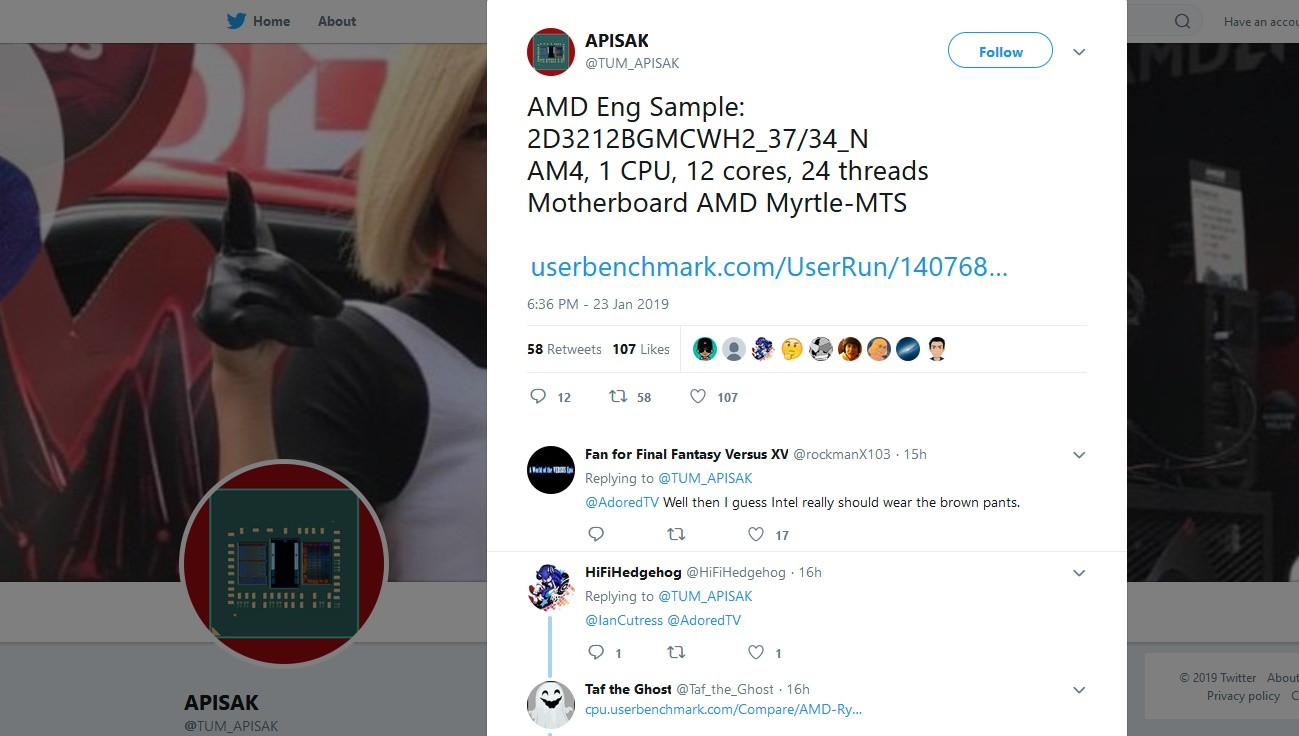
A new development could shake up our expectations on AMD's new Ryzen 2 CPUs, which if true, could mean that previous rumors of much increased core-counts at the top of AMD's offerings were true. User TUM Apisak, who has been involved in multiple information leaks and scouting for the hardware world, has digged enough to find a submitted UserBenchmark that screams of a 12-core, 24-thread AMD Matisse part (an engineering sample at that, so keep your hats on for the presented clock speeds).

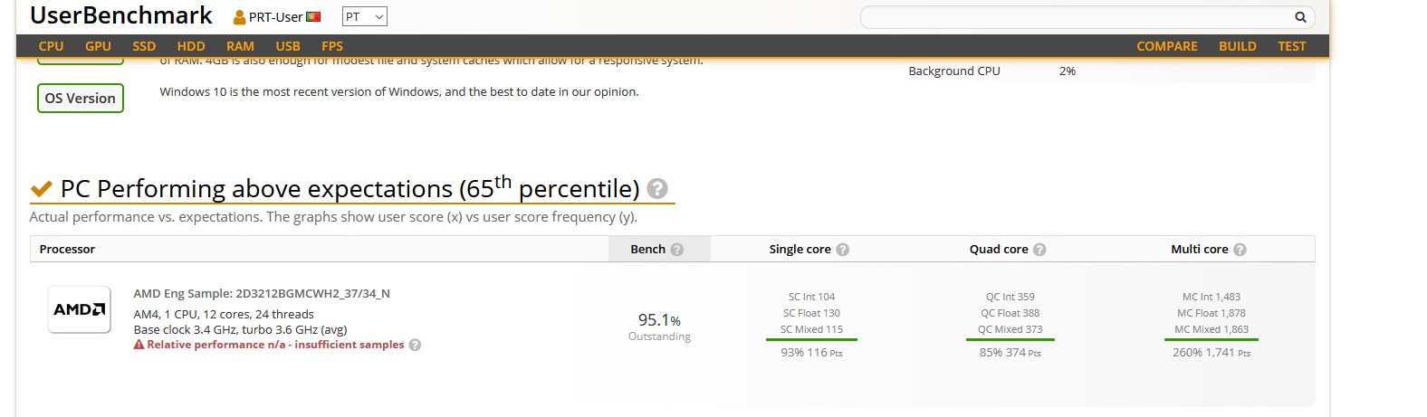
The benchmark list the used CPU via product code 2D3212BGMCWH2_37 / 34_N (H2 is indicative of a Matisse CPU The benchmark is listing a base clock speed of 3.4 GHz and an average boost clock speed of 3.6 GHz. The rest of the system specs are very, very basic, with 4 GB of 1333 MHz DDR4 memory being used on a new AMD platform, based on the Myrtle-MTS based chipset. The processor is listed having a 105 watts TDP and 32 MB of L3 cache.
Sources: TUM Apisak Twitter, User Benchmark
Add your own comment

35 Comments on AMD Zen 2 12-Core, 24-Thread Matisse CPU Spotted in UserBenchmark

#26
efikkan
All "leaks" like this that are genuine are intentional.
Posted on Reply
#27
Darmok N Jalad
It’s quite possible it’s intentional. It might be another case of a demo to compare to Intel’s best options. The CES demo was matching a 9900K’s performance for 50W less TDP. This one appears to match a 10C/20T 9900X in multicore for 60W less....on single channel DDR4 no less. Of course it’s just the one benchmark, but it also doesn’t appear to be AMD’s strongest possible effort based on the design.
Posted on Reply
#28
efikkan
I put this Zen 2 12-core up against the i9-9900X (10-core) in my table in post #6 for a reason; there are rumors of a stop-gap "Comet Lake" 10-core socket 1151 CPU until Ice Lake is fully here. If true, this will probably have similar characteristics of i9-9900X with some tweaks, and is probably the CPU the 12-core Zen 2 will be competing against.

While I do expect a final 12-core Zen 2 to be slightly higher clocked and get slightly better single and quad core scores, and the Zen 2 to have the upper hand in energy efficiency, I don't expect there to be a 60W difference in TDP. Let's hope Intel at least ditches the integrated graphics, it has nothing to do in a 10-core.

I do wonder though what place these CPUs deserve in the market. Don't get me wrong, options are fine and while they look compelling, what market demand do they serve?
It's obviously not gaming. And many heavy multithreaded workloads are also consuming of memory bandwidth. I guess these are relevant for people looking for a "HEDT lite", perhaps image editing or coding, but probably not heavy encoding or simulations. Personally I would probably not consider these high-core "mainstream" CPUs from either company, as I value the flexibility for more memory bandwidth and capacity, and when investing this much money anyway, the expandability of the platform is also something to consider.
Posted on Reply
#29
Darmok N Jalad
Skylake-X doesn’t have integrated graphics already. It also uses quad channel memory. Being a different design, I’m now sure how easy it will be for Intel to get it into their desktop socket. And that TDP value is for sustained all-core speed at base clock—turbo will take it way over 165W. I do actually expect there to be a big delta in TDP, as Zen2 is on 7nm and Skylake-X is 14nm. AMDs individual cores are actually pretty efficient—it’s the InfinityFabric that consumes a fair amount of power, especially when there is more than one CCX on a CPU. I’m curious if the chiplet design of Zen2 will improve this.
Posted on Reply
#30
efikkan
Darmok N JaladSkylake-X doesn’t have integrated graphics already. It also uses quad channel memory. Being a different design, I’m now sure how easy it will be for Intel to get it into their desktop socket. And that TDP value is for sustained all-core speed at base clock—turbo will take it way over 165W. I do actually expect there to be a big delta in TDP, as Zen2 is on 7nm and Skylake-X is 14nm.
A potential "Comet Lake" 10-core on socket 1151 will probably be an extended Skylake (non-X) design like the recent 8-core Coffee Lake refresh. My reasoning behind this is that the Skylake-X/SP 10-core design have a 6-channel memory controller, 2× UPI-links and AVX-512, all of which are "wasted" die space compared to the competition. But who knows, they have done strange things in the past.
Posted on Reply
#31
hat
Enthusiast
One might wonder whether the single stick of abysmally slow DDR4 has to do with showing off the CPU performance by using a terrible stick of RAM, or if they had to use that RAM to get the system to run...
Posted on Reply
#32
efikkan
DDR4-2667 isn't "abysmally slow".
I wouldn't read too much into the specifics of the setup as an indicator of problems with the platform. It's highly likely that this is some kind of validation setup, and the BIOS which was just a few days old might be an indicator of a BIOS or motherboard testing lab.
Posted on Reply
#33
ghazi
lexluthermiesterThat might be possible. Theoretically, that arrangement could have logistical, time and cost savings.
Correct me if I'm wrong, but I don't believe it's possible to have the L3 off-die with the current CCX design. My understanding is that the L3 is a fundamental part of making a CCX a CCX. Each has its own shared pool of L3 victim cache which is fully inclusive of the L2; cores within a CCX use the L3 to communicate with one another, and CCX's communicate with each other by transferring data between each others' L3 pools. Then there's the issue of latency which is already not very good with CCX design. We'll see though, it would make some amount of sense as caches are very costly in terms of die area and don't benefit much from node shrinks, and I suppose having the CCX's all use a single unified L3 could be considered an architectural advancement.
Posted on Reply
#34
Darmok N Jalad
ghaziCorrect me if I'm wrong, but I don't believe it's possible to have the L3 off-die with the current CCX design. My understanding is that the L3 is a fundamental part of making a CCX a CCX. Each has its own shared pool of L3 victim cache which is fully inclusive of the L2; cores within a CCX use the L3 to communicate with one another, and CCX's communicate with each other by transferring data between each others' L3 pools. Then there's the issue of latency which is already not very good with CCX design. We'll see though, it would make some amount of sense as caches are very costly in terms of die area and don't benefit much from node shrinks, and I suppose having the CCX's all use a single unified L3 could be considered an architectural advancement.
This is correct, at least with current Zen. We don’t really know how Zen 2 works yet. However, I’d be very surprised if Zen 2 deviated from this, as that would not only be a pretty significant design change, but it would also likely add latency to the the L3 and intercore communication, resulting in IPC decreases.
Posted on Reply
#35
efikkan
ghaziThen there's the issue of latency which is already not very good with CCX design. We'll see though, it would make some amount of sense as caches are very costly in terms of die area and don't benefit much from node shrinks, and I suppose having the CCX's all use a single unified L3 could be considered an architectural advancement.
Well, cache is one of the things that benefits the most from die shrinks. Cache is on the least thermally intensive end of the scale, which means it can be packed tighter, compared to FPUs, ALUs and register files which are on the opposite end of the scale. When it comes to packing cache tight, it comes more down to placement in terms of latency and in relation to the other parts of the design that needs to interact with it. So cache has traditionally been challenging to place due to its size and the increasing core complexity, but shrinks should generally help this.

I'm not sure making a unified L3 cache for several chiplets is a good idea in general, but not primarily because of latency as Darmok N Jalad mentioned, but because of the way L3 works. As you said, L3 is a victim cache, and in most designs it's an inclusive cache. There is a reason why Skylake-X changed this, because it's very inefficient use of die space, and it also means that increasing L2 will also decrease the efficiency of L3. As you probably know, modern CPUs typically split L1 cache into instruction and data caches, while L2 and L3 is both. And while L3 cache is shared between multiple cores, the actual sharing is commonly very minimal. The entire cache is overwritten every few microseconds, so the chance of two cores needing data from the same cache line is very minimal, because when you have multiple threads working, they have to use separate data, otherwise they would stall all the time. So the only thing that is generally shared between cores is instructions, if the cores are executing the same part of the code of course. And the few times the times the L3 victim cache is useful for data, it's usually from the same core that evicted it. So to sum up, L3 is largely wasteful in its current application, and only gives minor benefits.

I think it's time to re-evaluate L3 cache's role, and the changes Intel did in Skylake-X is probably just the beginning. Perhaps a split L3 cache, or instructions only L3 cache? Perhaps L3 shouldn't be shared and be data only, but L4 be instructions only and shared?
Posted on Reply
Add your own comment
Oct 5th, 2024 00:24 EDT change timezone

New Forum Posts

Popular Reviews

Controversial News Posts