Thursday, February 14th 2019

NVIDIA TU116 GPU Pictured Up Close: Noticeably Smaller than TU106
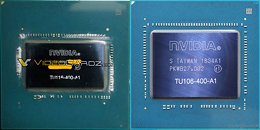
Here is the first picture of NVIDIA's 12 nm "TU116" silicon, which powers the upcoming GeForce GTX 1660 Ti graphics card. While the size of the package itself is identical to that of the "TU106" on which the RTX 2060 and RTX 2070 are based; the die of the TU116 is visibly smaller. This is because the chip physically lacks RT cores, and only has two-thirds the number of CUDA cores as the TU106, with 1,536 against the latter's 2,304. The die area, too, is about 2/3rds that of the TU106. The ASIC version of TU116 powering the GTX 1660 Ti is "TU116-400-A1."
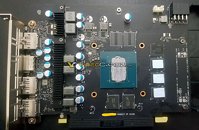
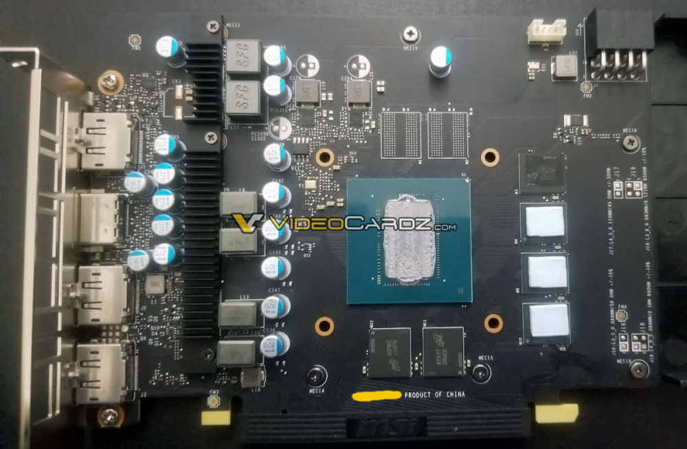
VideoCardz scored not just pictures of the ASIC, but also the PCB of an MSI GTX 1660 Ti Ventus graphics card, which reveals something very interesting. The PCB has traces for eight memory chips, across a 256-bit wide memory bus, although only six of them are populated with memory chips, making up 6 GB over a 192-bit bus. The GPU's package substrate, too, is of the same size. It's likely that NVIDIA is using a common substrate, with an identical pin-map between the TU106 and TU116, so AIC partners could reduce PCB development costs.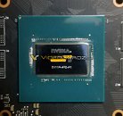

Source:
VideoCardz
VideoCardz scored not just pictures of the ASIC, but also the PCB of an MSI GTX 1660 Ti Ventus graphics card, which reveals something very interesting. The PCB has traces for eight memory chips, across a 256-bit wide memory bus, although only six of them are populated with memory chips, making up 6 GB over a 192-bit bus. The GPU's package substrate, too, is of the same size. It's likely that NVIDIA is using a common substrate, with an identical pin-map between the TU106 and TU116, so AIC partners could reduce PCB development costs.


35 Comments on NVIDIA TU116 GPU Pictured Up Close: Noticeably Smaller than TU106
Two Turing SMs with the same CUDA core count as one Pascal SM is ~60% bigger than Pascal.
My GTX 1060 is last year's technology but it is not dead yet.
Maybe later this year I will get a new card but I am in no rush.