Tuesday, October 6th 2020

AMD Big Navi GPU Features Infinity Cache?
As we are nearing the launch of AMD's highly hyped, next-generation RDNA 2 GPU codenamed "Big Navi", we are seeing more details emerge and crawl their way to us. We already got some rumors suggesting that this card is supposedly going to be called AMD Radeon RX 6900 and it is going to be AMD's top offering. Using a 256-bit bus with 16 GB of GDDR6 memory, the GPU will not use any type of HBM memory, which has historically been rather pricey. Instead, it looks like AMD will compensate for a smaller bus with a new technology it has developed. Thanks to the new findings on Justia Trademarks website by @momomo_us, we have information about the alleged "infinity cache" technology the new GPU uses.
It is reported by VideoCardz that the internal name for this technology is not Infinity Cache, however, it seems that AMD could have changed it recently. What does exactly you might wonder? Well, it is a bit of a mystery for now. What it could be, is a new cache technology which would allow for L1 GPU cache sharing across the cores, or some connection between the caches found across the whole GPU unit. This information should be taken with a grain of salt, as we are yet to see what this technology does and how it works, when AMD announces their new GPU on October 28th.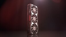
Source:
VideoCardz
It is reported by VideoCardz that the internal name for this technology is not Infinity Cache, however, it seems that AMD could have changed it recently. What does exactly you might wonder? Well, it is a bit of a mystery for now. What it could be, is a new cache technology which would allow for L1 GPU cache sharing across the cores, or some connection between the caches found across the whole GPU unit. This information should be taken with a grain of salt, as we are yet to see what this technology does and how it works, when AMD announces their new GPU on October 28th.

141 Comments on AMD Big Navi GPU Features Infinity Cache?
Here is a fair comparison: Crysis Remastered with vendor agnostic RT that can leverage RT cores on Turing
2070 Super is like 3x the performance of 5700XT when there is alot of RT effects there (2070 and 2070 Super is15% apart).
Right now against Ampere, the node advantage that Big Navi has is so tiny that it's not strange that Navi21 XT 530mm2 is competing against GA104 394mm2. Also Navi21 XT is a cut down version much like 3080. The full fat Navi21 XTX version will be reversed for the Pro version where AMD has better margin selling them.
The problem is however, that AMD has yet to even reach Turing's peak performance level, and not just by a few % either. You can afford 'a Turing' when you're ahead of the game, otherwise it just sets you back further. Let's be real about it: RDNA2 as it is dreamt to be, should've been here 1,5 year ago at the latest. The fact they're launching it now though is still good progress... like I said earlier. Time to market seems to have improved. If they can also get closer on absolute performance, I'll be cheering just as much as you.
The problem with Navi so far is that I have absolutely no reason for cautious optimism. AMD has been silent about it other than some vague percentages that really say as much as Ampere's very generously communicated 1.9x performance boost. As much as that number is far from credible.... why would this one suddenly be the truth? These claims have and will always be heavily inflated and best-case. Other than that, we do know AMD has severe limitations to work with, most notably on memory. Anyway... this has all been said before, but that's where I'm coming from here. Not an anti-AMD crusade... just realism and history of progress. I really want them to catch up, but I don't feel like the stars have aligned yet.
You're almost literally looking at a PS3 engine here. Single threaded.
My thoughts are different. I can almost see a repeat in "history" but not the one that negative-to-RDNA people see.
This could be a new ZEN case with RDNA1 to be the ZEN and RDNA2 to be ZEN2/3
I guess we will see in 20 days
"The increased R&D budget should help bolster AMD's graphics division for what comes after NAVI. The transition down to 7nm or 7nm+ for Nvidia will be a nice jump in performance though at the same time for them. What AMD has planned for what follows NAVI is somewhat critical. They can't let their foot off the gas and need to accelerate their plans a bit and be more aggressive.
AMD should probably aim for
- 3X more more instruction rate's over NAVI for it's successor
- 3X to 4X further lossless compression
- increase ROP's from 64 to 80
- improve the texture filter units by 0.5X
- improve texture mapping units by 0.5X to 1.5X (allowing for a better ratio of TFU's to TMU's)
- 3 CU resource pooling
- 7nm+ or node shrink
- more GDDR capacity hopefully I think by the time a successor arrives we could see more per chip GDDR6 capacity or a price reduction
- higher clocked GDDR
Bottom line I think AMD should really try to be more aggressive and further optimize it's efficiency of it's design and hopefully bump up frequency as well a bit. I don't think they need more stream processors right now, but rather need to improve the overall efficiency as a whole further to get more out of them. They also should aim to do some things to offer a few more GPU sku's to consumers at different price targets. I tend to think if they do that as well they might be able to even cut down chips to offer some good 2X or even 3X dual/triple GPU's as well based on PCIE 4.0 which good be good. I think if they could make the ROPs scale from 44/64/80 it would work well for just that type of thing and allowing better yields and binning options for AMD to offer to consumers.Those are my optimistic aggresive expectations of what AMD should try to aim towards for NAVI's successor if the R&D budget allows for it at least. They should really make some attempt to leap frog ahead a bit further especially as Nvidia will be shrinking down to a lower node for whatever comes after Turing or "SUPER" anyway since that sounds like more of a simply refresh and rebadge with a new bigger high end Super Titan sku added because what else would they name it instead 2080ti Super why!?!?"
Nvidia's GPU's are in general more granular in terms of workload management and thus power and efficiency. AMD needs to step it up more and it's not that AMD GPU's can't be efficient, but in order for a GPU like Vega 56/64 to compete with Nvidia's higher end and more diverse offers they have to stray more outside of power and efficiency so end up looking less efficient and more power hungry than they could be under more ideal circumstances with a better budget to design more complex and granular GPU's as Nvidia offers. It boils down to price segments and where they are marketed by both companies, but it's a more uphill battle for AMD given the R&D budget. The transition to 7nm was a smart call for AMD at least since it'll get cheaper over time along with yields and binning improvements. It should make for a easier transition to 7nm+ as well. Finer power gating would probably help out AMD a fair amount as well at improving TDP for load and idle and will become more important anyway at lower node sizes to reduce voltages and waste heat plus it's important for mobile which is a area for big room for growth for the company."
It was mostly just goal posts to aim toward, but should be intriguing to see where AMD went with the design obviously they had a bit of a basis with RDNA and by extension GNC and everything before them. Looking at it today 64/80 ROPs card seem plausible while 44ROPs is highly doubtful, but it was even then even with a mGPU scenario it would be rather unlikely still who knows maybe they surprise us. Though if they were doing a mGPU solution I'd think they incorporate the infinity fabric bridge that Radeon Pro workstation card came up with as well as the infinity cache that's rumored the combination would probably do a lot to reduce and minimize the latency micro-stutter matter.
Looking at it now I tend to think a 72 ROPs and possibly 88 ROPs card is plausible to consider. If they can carve out a 64/72/80 ROPs segmentation that would probably be decent having 4 cards in total. Given the amount of SKU's Nvidia often offers that could be good for AMD. The interesting part about a 88ROPs sku is they could bin those chips and saving them aside and hold out to utilize them with GGDR6X a little further down the road when pricing for that normalizes and/or capacity increases. If they do it that way with the ROPs I could see a 224-bit/256-bit/288-bit/320-bit memory bus options plausible with infinity cache balancing them out further.
To me it looks like they are sticking to a single chip solution so probably bolstered the ROPs a fair bit along with some of those other area's mentioned. I think the highest end SKU will end up with either 80 or 88 ROPs it might initially be 80ROPs with some premium 88ROPs SKU's being binned and tucked away for a rainy day perhaps though tough to say. What rabbits will AMD pull out of it's hat of mysteries!!? Who knows though certainly fun to speculate though. I do hope they took some of those bullet points into consideration.
Improving the compression would be big deal I think they've fallen behind in that area relative to Nvidia. Some of the other stuff I felt with offer some synchronizing benefits along with improved design performance and/or efficiency enhancements. I think I looked at VEGA and RNDA block design diagrams to get a basic idea and figure out just how they might take things steps further for RDNA2 based on the changes made between VEGA to RDNA and some of my own personal injections. To me it was quite obvious they were trailing Nvidia and needed to hopefully make a big push on RDNA2 given Nvidia is already going to have a nice performance aid from the chip die shrink.
I feel like over engineering RNDA2 is the only practical way AMD can claw it's way back ahead of Nvidia especially this GPU refresh round since they were already at 7nm though idk if RNDA2 will be 7nm+ or not which would help and be welcome naturally. Nvidia will likely have higher priority on GDDR6X as well for sometime. In a sense and with AMD probably knowing Nvidia probably end up with a higher priority on that newer memory type that lends some credibility to the possibility of a infinity cache to offset it especially if they combine it with a slightly wider memory bus width. To me a big key is how well they segment the different GPU SKU's. On the memory side there are different scenario's at play do they have some SKU's with more ROP's and a wider memory bus with GDDR6X or HBM2!? Is the infinity cache scaled depending on SKU and how big is it and is it availible for all SKU's? Lots of possibilities and what are they doing with compression I sure hope they are making inroads to improve that.
HD 7970 vs GTX 680 (264GBps vs 192GBps)
R9 290X vs GTX 780 Ti (320GBps vs 336GBps)
Fury X vs 980 Ti (512GBps vs 336 GBps)
Vega64 vs 1080 Ti (484GBps vs 484GBps)
RadeonVII vs 2080Ti (1024GBps vs 616GBps)
5700XT vs 2080 (448GBps vs 448GBps)
And now you think AMD can just make a card with 448GBps bandwidth that can compete with a 760GBps card from Nvidia. Keep on dreaming buddy, or play AoTS.
AMD was really hoping Nvidia would name the GA104 as the 3080 just like they did the 2080, but nope Nvidia is serious about burying the next Gen consoles this time around.
GTX 680: 256 bit, 192.3 GB/s
With ~27% less memory bandwidth GTX 680 could compete with HD 7970.
R9 390X: 512 bit, 384.0 GB/s
GTX 980: 256 bit, 224.4 GB/s
With ~42% less memory bandwidth GTX 980 could more than just compete with RX 390X.
RX Vega 64: 2048 bit, 483.8 GB/s
GTX 1080: 256 bit, 320.3 GB/s
With ~34% less memory bandwidth GTX 1080 could compete with RX Vega 64.
You see, bandwidth alone doesn't say much. You have to get the whole picture. RTX 3080 has a bandwidth of 760.3 GB/s. Big Navi is expected to have a bandwidth of >500 GB/s. Which might be something like 30-35% less bandwidth than 3080. But as you can see, you can compete with even such a deficit if your architecture is well optimized.
Well, tell us more and give us the spoils! This is indeed entertaining.
Besides, what you're saying is true but AMD doesn't have the Nvidia headstart of better delta compression (980, 1080) at any point in time. Its not optimization, its feature set that made that possible.
Also, the 7970 did age a whole lot better, as in several years of actual practical use out of it, than the 680. Not directly due to bandwidth, but capacity. In none of the three examples is bandwidth the true factor making the difference, really. Nvidia just had a much stronger architecture across the board from Maxwell onwards.
As to your first point, AMD might very well have improved their delta color compression so much that it beats Nvidia's, but if so that wouldn't negate the fact that Nvidia has had the advantage there for four+ generations. That would of course make overtaking them all the more impressive, but your argument has fundamental logical flaws.
Raw compute is pretty pointless when a competitor dominates the market with optimized CUDA workloads anyway. So even outside of gaming, wtf are you even on about. Spec sheets dont get work done last I checked.
Okay, then how about some facts. You said RDNA 2 won't fight the 3080 with that bandwidth. Give us some facts about RDNA 2 why it won't happen. No opinions, no referring to old GCN stuff, just hard facts about RDNA.
Besides that, you're still ignoring efficiency. Let's start back in 2013:
Radeon 290X: $550, 5.6TFlops, 438mm² (12.8Gflops/mm²), 290W (19.3Gflops/W), 100% gaming performance.
Geforce GTX 780 Ti: $699, 5.3Tflops, 561mm ² (9.4Gflops/mm²), 250W (21.2Gflops/W), 104% gaming performance
Radeon Fury X: $699, 8.6TFlops, 596mm² (14.4Gf/mm²), 275W (31.3Gflops/W), 131% gaming performance
Geforce GTX 980 Ti: $699, 6.1Tflops, 601mm² (10.1Gf/mm²), 250W (24,4Gflops/W), 133% gaming performance
Radeon Vega 64: $499, 12.7Tflops, 495mm² (25.7Gf/mm²), 295W (43.1Gflops/W), 173% gaming performance
Geforce GTX 1080 Ti: $699, 11.3Tflops, 471mm² (24Gf/mm²), 250W (45.2Gflops/W), 223% gaming performance.
So, what was AMD good at? Delivering FP32 compute for cheap (compared to Nvidia). For some generations they kept pace in terms of gaming performance too, but always at the cost of higher power, and in the Fury X (still using mine!) and onwards that's partially thanks to exotic and expensive memory that's dramatically more efficient than GDDR. They also delivered quite good compute per die area. In gaming they kept up at best, lagged behind dramatically at worst (though then also at a lower price).
What can we extrapolate from this? That GCN was a good architecture for compute. It was very clearly a worse architecture than what Nvidia had to offer overall, as compute is not the major relevant use case for any consumer GPU. So, in any perspective other than that of someone running a render farm, AMD's architecture was clearly worse than Nvidia's.
This is very clearly demonstrated by RDNA: The 5700 XT matches the Radeon VII in gaming performance despite a significant drop in compute performance. It also dramatically increases gaming performance/W, though compute/W is down from the VII.But you did. You said AMD had a "much stronger architecture" until Pascal. Which means that you're arguing that compute is more important than gaming performance, as that is the only metric in which they were better. Yet you're in a discussion about whether RDNA 2 can match or beat Ampere in gaming performance based on rumored memory bandwidths, arguing against someone skeptical of this. While we know that RDNA is a worse architecture for compute than GCN, watt for watt on the same node, and you're arguing for RDNA 2 likely being very good - which implies that more gaming performance = better. So whether you meant there to be or not, there is a distinct reference point shift between those two parts of your arguments.
Let me sum it up for you again. That's what I said:And that's what you saidWhich is the very same statement. Just expressed in other words.
You are presenting an argument from a point of view where the "strength" of a GPU architecture is apparently only a product of its FP32 compute prowess. I am presenting a counterargument saying that this is a meaningless measure for home/enthusiast uses, both due to your argument ignoring efficiency (which is always relevant when discussing an architecture, as better efficiency = more performance in a given power envelope) and due to FP32 compute being of relatively low importance to this user group. You are also for some reason equating FP32 compute to "raw performance", which is a stretch given the many tasks a GPU can perform. FP32 is of course one of the more important ones, but it alone is a poor measure of the performance of a GPU, particularly outside of enterprise use cases.
Put more simply: you are effectively saying "GCN was a good architecture, but bad at gaming" while I am saying "GCN was a mediocre architecture, but good at compute." The point of reference and meaning put into what amounts to a good architecture in those two statements are dramatically different. As for saying "strong" rather than "good" or whatever else: these are generic terms without specific meanings in this context. Trying to add a post-hoc definition doesn't make the argument any more convincing.
ZEN3 architecture is all ZEN... Started with ZEN >> ZEN+ >>ZEN2 continuously improving and yet again they manage to enhance it on the exact same node and improve IPC and performance per watt all together. RDNA2 is just a step back (=ZEN2) and it will bring impovements. RDNA3 will prabably be like a ZEN3 iteration.
PolarisPascal. That's why I think splitting up the architecture into RDNA and CDNA was the right decision. It's a little bit like Skylake. Skylake was a really good architecture on release. But over the years there was no real improvement. Only higher clock speed and higher power consupmtion. OTOH AMD mode significant progress with every new full Zen generation.How about answering my question first? I'm still missing that one.